FDN028N20 Overview
Key Specifications
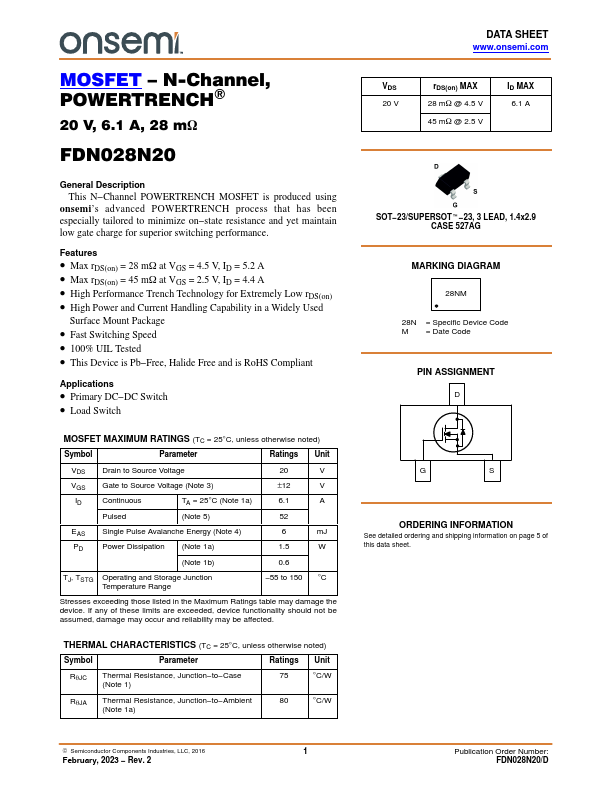
Package: SOT-23-3
Mount Type: Surface Mount
Height: 1.12 mm
Max Operating Temp: 150 °C
Description
This N-Channel POWERTRENCH MOSFET is produced using onsemi’s advanced POWERTRENCH process that has been especially tailored to minimize on-state resistance and yet maintain low gate charge for superior switching performance.
Key Features
- Max rDS(on) = 28 mW at VGS = 4.5 V, ID = 5.2 A
- Max rDS(on) = 45 mW at VGS = 2.5 V, ID = 4.4 A
- High Performance Trench Technology for Extremely Low rDS(on)
- High Power and Current Handling Capability in a Widely Used Surface Mount Package
- Fast Switching Speed