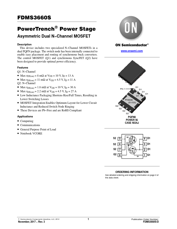
FDMS3660S
Overview
- Max rDS(on) = 8 mW at VGS = 10 V, ID = 13 A
- Max rDS(on) = 11 mW at VGS = 4.5 V, ID = 11 A Q2: N-Channel
- Max rDS(on) = 1.8 mW at VGS = 10 V, ID = 30 A
- Max rDS(on) = 2.2 mW at VGS = 4.5 V, ID = 27 A
- Low Inductance Packaging Shortens Rise/Fall Times, Resulting in Lower Switching Losses
- MOSFET Integration Enables Optimum Layout for Lower Circuit Inductance and Reduced Switch Node Ringing
- These Devices are Pb-Free and are RoHS Compliant