The following content is an automatically extracted verbatim text
from the original manufacturer datasheet and is provided for reference purposes only.
View original datasheet text
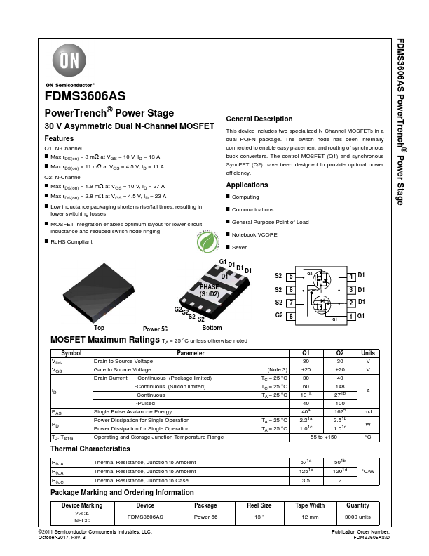
FDMS3606AS PowerTrench® Power Stage
FDMS3606AS
PowerTrench® Power Stage
30 V Asymmetric Dual N-Channel MOSFET
Features
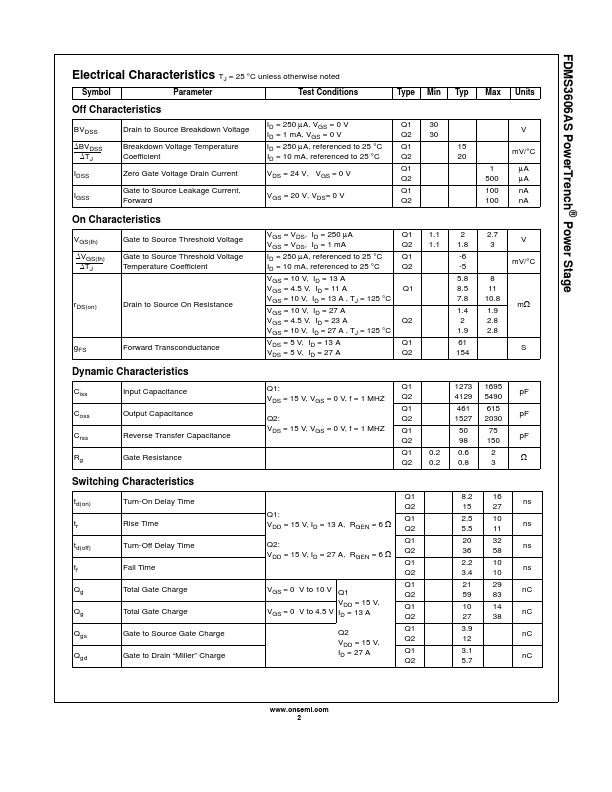
Q1: N-Channel Max rDS(on) = 8 mΩ at VGS = 10 V, ID = 13 A Max rDS(on) = 11 mΩ at VGS = 4.5 V, ID = 11 A Q2: N-Channel Max rDS(on) = 1.9 mΩ at VGS = 10 V, ID = 27 A Max rDS(on) = 2.8 mΩ at VGS = 4.5 V, ID = 23 A Low inductance packaging shortens rise/fall times, resulting in
lower switching losses
MOSFET integration enables optimum layout for lower circuit inductance and reduced switch node ringing
RoHS Compliant
General Description
This device includes two specialized N-Channel MOSFETs in a dual PQFN package. The switch node has been internally connected to enable easy placement and routing of synchronous buck converters.
 FDMS3606AS Datasheet