Datasheet4U Logo Datasheet4U.com

FDD2670 - N-Channel MOSFET

Datasheet Summary

Description

This N-Channel MOSFET has been designed specifically to improve t he overall efficiency of DC/DC converters using either synchronous or conventional switching PWM controllers.

These MOSFET's feature faster switching and lower gate charge than other MOSFET's with comparable RDS(ON) specifications.

Features

  • 3.6 A, 200 V. RDS(ON) = 130 mΩ @ VGS = 10 V.
  • Low gate charge.
  • Fas t switching speed.
  • High performance trench technology for extremely low RDS(ON).
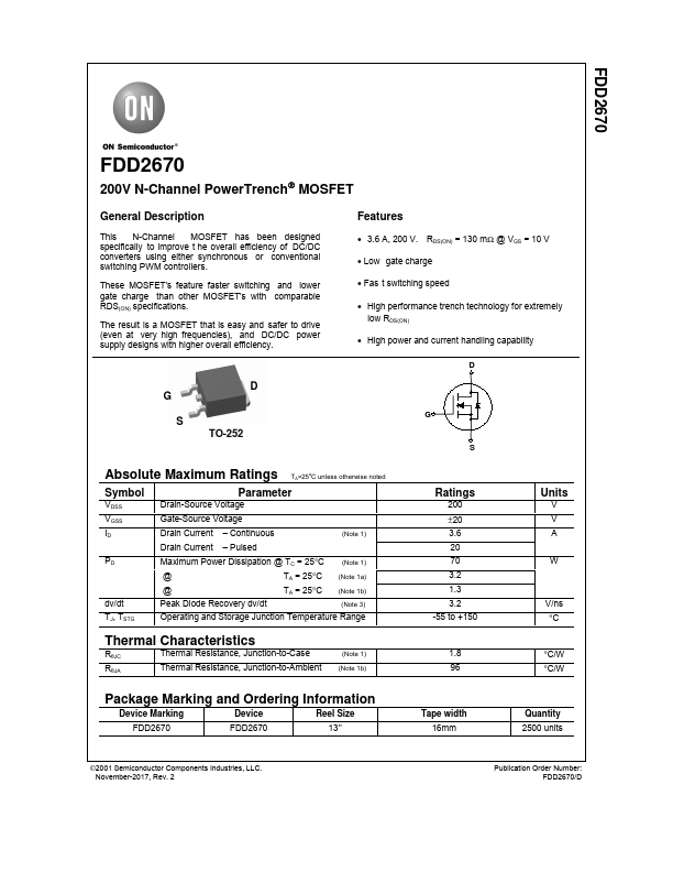
  • High power and current handling capability D G S Absolute Maximum Ratings TA=25oC unless otherwise noted Symbol VDSS VGSS ID Parameter Drain-Source Voltage Gate-Source Voltage Drain Current.
  • Continuous Drain Current.
  • Pulsed (Note 1) PD dv/dt Maximum Power Dissipation @ TC = 25°C @.

📥 Download Datasheet

Datasheet preview – FDD2670

Datasheet Details

Part number FDD2670
Manufacturer ON Semiconductor
File Size 378.47 KB
Description N-Channel MOSFET
Datasheet download datasheet FDD2670 Datasheet
Additional preview pages of the FDD2670 datasheet.
Other Datasheets by ON Semiconductor

Full PDF Text Transcription

Click to expand full text
FDD2670 FDD2670 200V N-Channel PowerTrench MOSFET General Description This N-Channel MOSFET has been designed specifically to improve t he overall efficiency of DC/DC converters using either synchronous or conventional switching PWM controllers. These MOSFET's feature faster switching and lower gate charge than other MOSFET's with comparable RDS(ON) specifications. The result is a MOSFET that is easy and safer to drive (even at very high frequencies), and DC/DC power supply designs with higher overall efficiency. D G S TO-252 Features • 3.6 A, 200 V.
Published: |