FDC6420C
FDC6420C is Dual-Channel MOSFET manufactured by onsemi.
MOSFET
- N & P-Channel, POWERTRENCH)
20 V
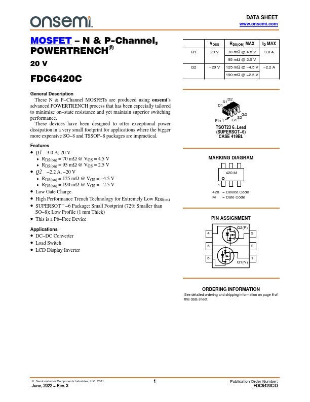
General Description These N & P- Channel MOSFETs are produced using onsemi’s advanced POWERTRENCH process that has been especially tailored to minimize on- state resistance and yet maintain superior switching performance.
These devices have been designed to offer exceptional power dissipation in a very small footprint for applications where the bigger more expensive SO- 8 and TSSOP- 8 packages are impractical.
Features
- Q1 3.0 A, 20 V
- RDS(on) = 70 m W @ VGS = 4.5 V
- RDS(on) = 95 m W @ VGS = 2.5 V
- Q2
- 2.2 A,
- 20 V
- RDS(on) = 125 m W @ VGS =
- 4.5 V
- RDS(on) = 190 m W @ VGS =
- 2.5 V
- Low Gate Charge
- High Performance Trench Technology for Extremely Low RDS(on)
- SUPERSOTt- 6 Package: Small Footprint (72% Smaller than
SO- 8); Low Profile (1 mm Thick)
- This is a Pb- Free Device
Applications
- DC- DC Converter
- Load Switch
- LCD Display Inverter
DATA SHEET .onsemi.
VDSS
RDS(ON) MAX ID MAX
Q1
20 V 70 m W @ 4.5 V 3.0...