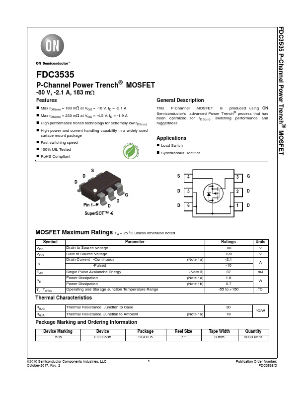
Datasheet4U Logo Datasheet4U.com

FDC3535 Datasheet P-Channel MOSFET

Manufacturer: onsemi

Overview: FDC3535 P-Channel Power Trench® MOSFET FDC3535 P-Channel Power Trench® MOSFET -80 V, -2.

General Description

„ Max rDS(on) = 183 mΩ at VGS = -10 V, ID = -2.1 A „ Max rDS(on) = 233 mΩ at VGS = -4.5 V, ID = -1.9 A „ High performance trench technology for extremely low rDS(on) „ High power and current handling capability in a widely used surface mount package „ Fast switching speed „ 100% UIL Tested „ RoHS Compliant This P-Channel MOSFET is produced using ON Semiconductor‘s advanced Power Trench® process that has been optimized for rDS(on), switching performance and ruggedness.

Applications „ Load Switch „ Synchronous Rectifier S D D Pin 1 G D D SuperSOTTM -6 S4 D5 D6 3G 2D 1D MOSFET Maximum Ratings TA = 25 °C unless otherwise noted Symbol VDS VGS ID EAS PD TJ, TSTG Parameter Drain to Source Voltage Gate to Source Voltage Drain Current -Continuous -Pulsed Single Pulse Avalanche Energy Power Dissipation Power Dissipation Operating and Storage Junction Temperature Range Thermal Characteristics (Note 1a) (Note 3) (Note 1a) (Note 1b) Ratings -80 ±20 -2.1 -10 37 1.6 0.7 -55 to +150 Units V V A mJ W °C RθJC RθJA Thermal Resistance, Junction to Case Thermal Resistance, Junction to Ambient Package Marking and Ordering Information 30 (Note 1a) 78 °C/W Device Marking .535 Device FDC3535 Package SSOT-6 Reel Size 7 ’’ Tape Width 8 mm Quantity 3000 units ©2010 Semiconductor Components Industries, LLC.

1 October-2017, Rev.

Key Features

  • General.