CS5205-3
Key Features
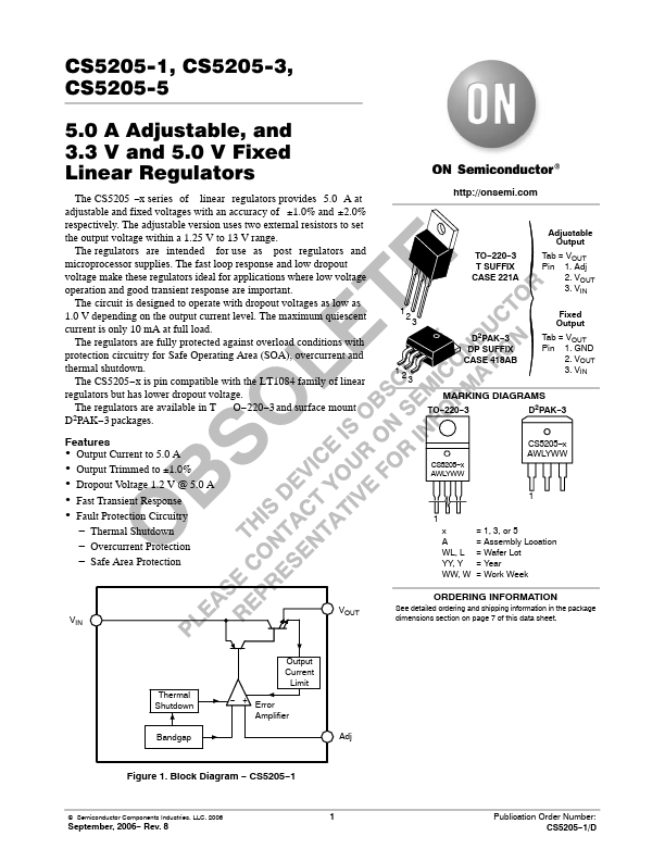
- Output Current to 5.0 A
- Output Trimmed to ±1.0%
- Dropout Voltage 1.2 V @ 5.0 A
- Fast Transient Response
- Fault Protection Circuitry - Thermal Shutdown - Overcurrent Protection - Safe Area Protection
| Part Number | Manufacturer | Description |
|---|---|---|
| CS5205-1 | Cherry Semiconductor Corporation | 5A Adjustable/ and 3.3V and 5V Fixed Linear Regulators |
| CS5205-3 | Cherry Semiconductor Corporation | 5A Adjustable/ and 3.3V and 5V Fixed Linear Regulators |
| CS5205-5 | Cherry Semiconductor Corporation | 5A Adjustable/ and 3.3V and 5V Fixed Linear Regulators |