CS5204-1
CS5204-1 is Linear Regulators manufactured by onsemi.
Features
.. http://onsemi.
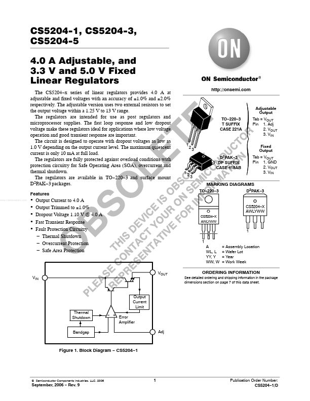
Adjustable Output TO- 220- 3 T SUFFIX CASE 221A Tab = VOUT Pin 1. Adj 2. VOUT 3. VIN Fixed Output D2PAK- 3 DP SUFFIX CASE 418AB 12 3 TO- 220- 3 Tab = VOUT Pin 1. GND 2. VOUT 3. VIN
MARKING DIAGRAMS
D2PAK- 3
- -
- -
- Output Current to 4.0 A Output Trimmed to ±1.0% Dropout Voltage 1.10 V @ 4.0 A Fast Transient Response Fault Protection Circuitry
- Thermal Shutdown
- Overcurrent Protection
- Safe Area Protection
CS5204- X AWLYWW
CS5204- X AWLYWW
1 1 A WL, L YY, Y WW, W VOUT = Assembly Location = Wafer Lot = Year = Work Week
ORDERING INFORMATION
See detailed ordering and shipping information in the package dimensions section on page 7 of this data sheet.
Output Current Limit Thermal Shutdown Bandgap
- + Error Amplifier Adj
Figure 1. Block Diagram
- CS5204- 1
© Semiconductor ponents Industries, LLC, 2006
September, 2006
- Rev. 9
Publication Order Number: CS5204- 1/D
CS5204- 1, CS5204- 3, CS5204- 5
VOUT
Output Current Limit Thermal Shutdown
- + Error Amplifier
Bandgap GND
Figure 2. Block Diagram
- CS5204- 3,
- 5 MAXIMUM RATINGS-
Parameter Supply Voltage, VCC Operating Temperature Range Junction Temperature Storage Temperature Range Lead Temperature Soldering: 1. 10 second maximum. 2. 60 second maximum above 183°C.
- The maximum package power dissipation must be observed. Wave Solder (through hole styles only) Note 1 Reflow (SMD styles only) Note 2 Value...