Datasheet4U Logo Datasheet4U.com

CS1112 - Quad Power Output Driver

Description

PACKAGE PIN # 24 Lead SOIC 1 2 3 4 5, 6, 7, 8 17, 18, 19, 20 9 10 11 12 13 14 PIN SYMBOL VDD VPWR OUT0 IN0 GND IN1 OUT1 SI CSB SCLK SO FUNCTION Input voltage to bias logic and control circuitry.

Input voltage to bias gate drive circuitry.

Open drain output one.

Features

  • 4.0 MHz Serial Input Bus Parallel Input Control 1.0 Ω DMOS Drivers (typ) Power On Reset Internal Flyback Clamps Status Output Fault Protection.
  • 46 V Peak Transient.
  • Power Limiting.
  • Undervoltage.
  • Overvoltage.
  • Fault Reporting.
  • Open Load.
  • Short Circuit.
  • 8 Internally Fused Leads
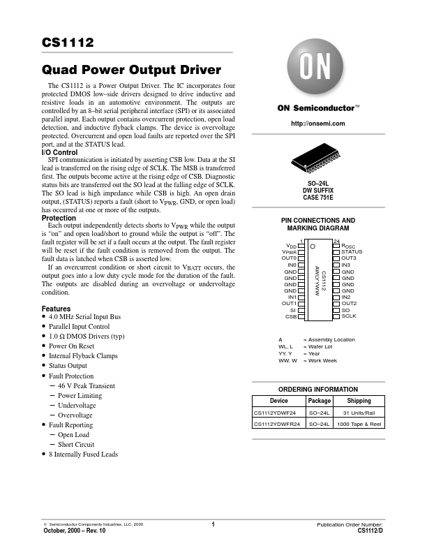
 http://onsemi. com SO.
  • 24L DW SUFFIX CASE 751E PIN.

📥 Download Datasheet

Datasheet Details

Part number CS1112
Manufacturer onsemi
File Size 93.65 KB
Description Quad Power Output Driver
Datasheet download datasheet CS1112 Datasheet

Full PDF Text Transcription (Reference)

The following content is an automatically extracted verbatim text from the original manufacturer datasheet and is provided for reference purposes only.

View original datasheet text
CS1112 Quad Power Output Driver The CS1112 is a Power Output Driver. The IC incorporates four protected DMOS low–side drivers designed to drive inductive and resistive loads in an automotive environment. The outputs are controlled by an 8–bit serial peripheral interface (SPI) or its associated parallel input. Each output contains overcurrent protection, open load detection, and inductive flyback clamps. The device is overvoltage protected. Overcurrent and open load faults are reported over the SPI port, and at the STATUS lead. I/O Control SPI communication is initiated by asserting CSB low. Data at the SI lead is transferred on the rising edge of SCLK. The MSB is transferred first. The outputs become active at the rising edge of CSB.
Published: |