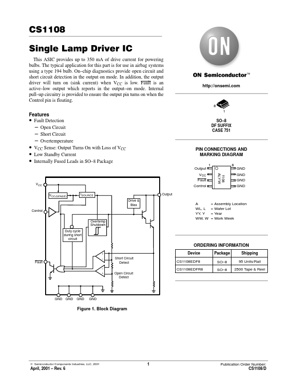
CS1108
MAXIMUM RATINGS*
Rating
Storage Temperature
VCC, Fault, Control
ESD Capability (Human Body Model)
Peak Transient Voltage (output off mode, output pin only)
Lead Temperature Soldering:
1. 60 second maximum above 183°C.
*The maximum package power dissipation must be observed.
(26 V Load Dump @ 14 V VBAT)
Reflow: (SMD styles only) (Note 1)
Value
–65 to +150
–0.5 to 6.0
2.0
40
230 peak
Unit
°C
V
kV
V
°C
ELECTRICAL CHARACTERISTICS (4.75 ≤ VCC ≤ 5.25 V, –40°C ≤ TA ≤ 85°C, –40°C ≤ TJ ≤ 150°C; unless other-
wise specified.)
Characteristic
Test Conditions
Min Typ Max
Supply Requirements
VCC Quiescent Current
Output
Output ON
Output OFF
– 3.0 6.0
– 100 250
Leakage Current
Saturation Voltage
VOUTPUT (self–bias)
Current Sense
Short Circuit Current
VBAT = 14 V
IOUTPUT = 350 mA
IOUTPUT = 180 mA
VCC < 4.5 V, IOUTPUT < 200 mA
–
– 16 100
– 1.1 1.5
– 0.9 1.3
– – 3.5
350 500 650
Open Circuit Current
Output in the ON state
20 40 60
Control–Input
Input Voltage
Logic = High
Logic = Low
2.0 –
–
– – 0.8
Input Current
Logic = VCC
Logic = 0 V
– 20
–50 –20
40
–
Fault Output – (Open Collector)
Output Low Voltage
IFAULT = 250 µA (sink)
– 0.24
Overtemperature Shutdown
TJ Output Disable Threshold
(Guaranteed by Design)
150 180
TJ Hysteresis
(Guaranteed by Design)
5.0 –
Note: A fault signal will be shown (at the fault pin) during inrush as the short circuit threshold is exceeded.
0.40
–
–
Unit
mA
µA
µA
V
V
V
mA
mA
V
V
µA
µA
V
°C
°C
PACKAGE PIN DESCRIPTION
PACKAGE PIN #
8 Lead SO Narrow
1
2
3
4
5, 6, 7, 8
PIN SYMBOL
Output
VCC
Fault
Control
Ground
FUNCTION
Open collector output.
5.0 V regulated supply input.
Open collector diagnostic output low during open load, short
circuit and overtemperature conditions.
TTL compatible input.
Signal ground.
http://onsemi.com
2