CS1107 Overview
Key Features
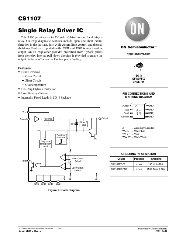
- Fault Detection – Open Circuit – Short Circuit – Overtemperature
- On–Chip Flyback Protection
- Low Standby Current
| Part | CS1107 |
|---|---|
| Description | Single Relay Driver |
| Manufacturer | onsemi |
| Size | 70.88 KB |
| Part Number | Manufacturer | Description |
|---|---|---|
| CS1107 | Cherry Semiconductor Corporation | Single Relay Driver |
| CS1102 | Unknown Manufacturer | CIT SWITCH |
| CS1108 | Cherry Semiconductor Corporation | Single Lamp Driver |
| CS110N06A8-2 | CR Micro | Silicon N-Channel Power MOSFET |
| CS1101 | CIT Relay | DIMENSIONS SCHEMATIC & PC LAYOUT |