The following content is an automatically extracted verbatim text
from the original manufacturer datasheet and is provided for reference purposes only.
View original datasheet text
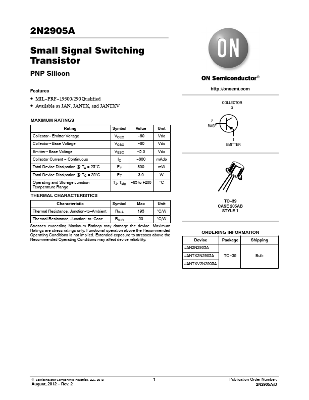
2N2905A
Small Signal Switching Transistor
PNP Silicon
Features
• MIL−PRF−19500/290 Qualified • Available as JAN, JANTX, and JANTXV
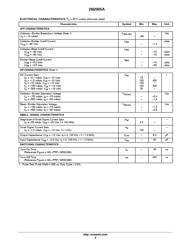
MAXIMUM RATINGS
Rating Collector −Emitter Voltage Collector −Base Voltage Emitter −Base Voltage Collector Current − Continuous Total Device Dissipation @ TA = 25°C Total Device Dissipation @ TC = 25°C Operating and Storage Junction Temperature Range
Symbol Value
VCEO
−60
VCBO
−60
VEBO IC
−5.0 −600
PT 800
PT 3.0
TJ, Tstg −65 to +200
Unit Vdc Vdc Vdc mAdc mW W °C
THERMAL CHARACTERISTICS
Characteristic
Symbol
Max
Unit
Thermal Resistance, Junction−to−Ambient RqJA
195 °C/W
Thermal Resistance, Junction−to−Case
RqJC
50 °C/W
Stresses exceeding Maximum Ratings may damage the device. Maximum Ratings are stress ratings only.
 2N2905A Datasheet