2N2222
2N2222 is NPN Amplifier Transistor manufactured by onsemi.
Features
- These are Pb- Free Devices-
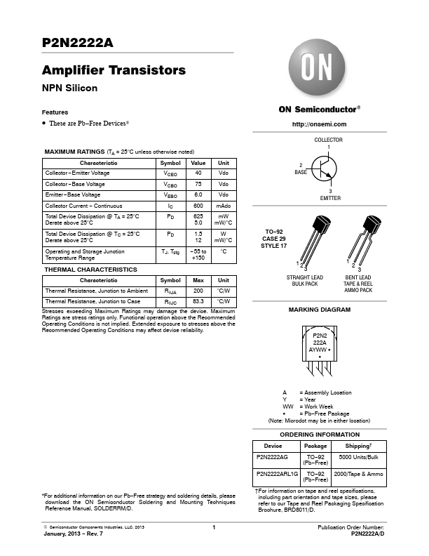
MAXIMUM RATINGS (TA = 25°C unless otherwise noted)
Characteristic
Symbol Value
Collector
- Emitter Voltage
VCEO
Collector
- Base Voltage
VCBO
Emitter- Base Voltage
VEBO
Collector Current
- Continuous Total Device Dissipation @ TA = 25°C Derate above 25°C
Unit Vdc Vdc Vdc m Adc m W m W/°C
Total Device Dissipation @ TC = 25°C Derate above 25°C
12 m W/°C
Operating and Storage Junction Temperature Range
TJ, Tstg
- 55 to
°C
+150
THERMAL CHARACTERISTICS
Characteristic
Symbol Max Unit
Thermal Resistance, Junction to Ambient
Rq JA
200 °C/W
Thermal Resistance, Junction to Case
Rq JC
83.3 °C/W
Stresses exceeding Maximum Ratings may damage the device. Maximum Ratings are stress ratings only. Functional operation above the Remended Operating Conditions is not implied. Extended exposure to stresses above the Remended Operating Conditions may affect device reliability. http://onsemi.
COLLECTOR 1
2...

Representative 2N2222 image (package may vary by manufacturer)