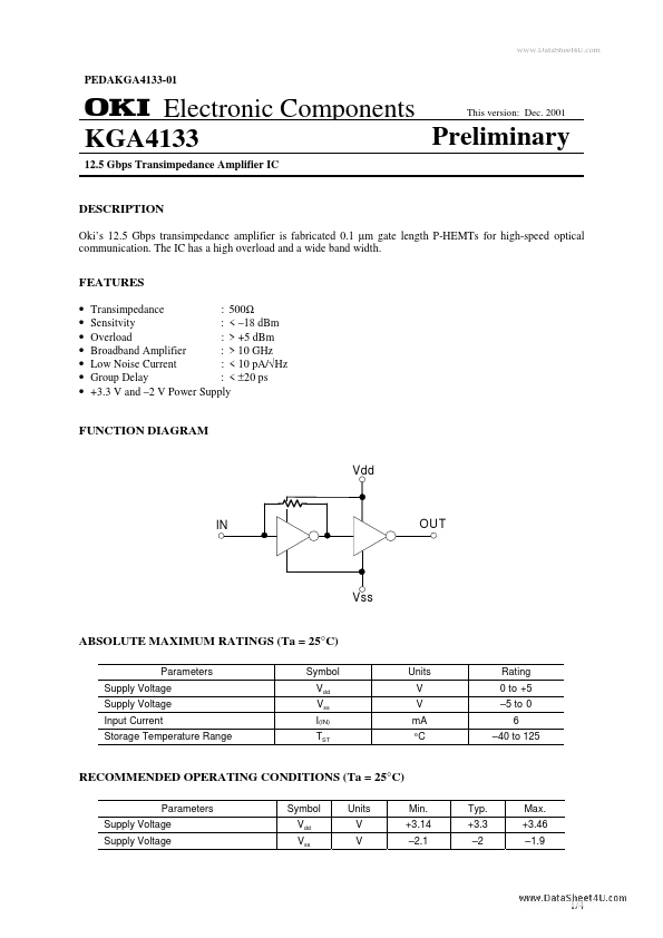
1Electronic Components
www.DataSheet4U.com
PEDAKGA4133-01
KGA4133
ELECTRICAL CHARACTERISTICS
Parameters
(Ta = 25°C, Vdd = +3.3 V, VSS = –2 V, C(diode)+C(stray) = 0.20 pF)
Units
Min.
Typ.
Max.
Transimpedance (I(IN)<450 µA)
Bandwidth (–3 dB)
Ω — 500 —
GHz 10 10.5 —
Transimpedance Flatness (300 kHz to 6 GHz)
dBΩ
—
—
±1
Equivalent Input Noise Current
*1) pA/√Hz
—
9.5
—
Optical Sensitivity
*2) dBm
—
–18
—
Optical Overload
*2) dBm
—
+5 —
Input Offset Voltage
V — +0.16 —
Group Delay
ps — — ±20
Output Return Loss (<10 GHz)
dB — — 10
Power Consumption
W — 0.22 —
Operating Temperature Range
*3) °C 0 — +85
*1) Averaged Equivalent Input Noise Current from 130 MHz to 9.0 GHz.
*2) Value of optical sensitivity is guaranteed by design, assuming responsivity of photo diode of 0.90 A/W.
*3) At backside of die.
EYE DIAGRAMS
(12.5 Gbps PRBS 231-1 Input signal)
Optical Input Power= -17[dBm]
Optical Input Power = -10[dBm]
(20ps/div)
Optical Input Power = 0[dBm]
(20ps/div)
Optical Input Power = +5[dBm]
(20ps/div)
(20ps/div)
2/4