MR26V25655J
MR26V25655J is 8M-Word x 32Bit or 64M-Word x 16Bit P2ROM manufactured by OKI Electric.
FEATURES
- 8,388,608-word × 32-bit/16,777,216-word × 16-bit electrically switchable configuration
- Page size of 8-word x 32-Bit or 16-word x 16-Bit
- 3.0 V to 3.6 V power supply
- Random Access time 120 ns MAX
- Page Access time 35 ns MAX
- Operating current 100 m A MAX
- Standby current 50 µA MAX
- Input/Output TTL patible
- Three-state output
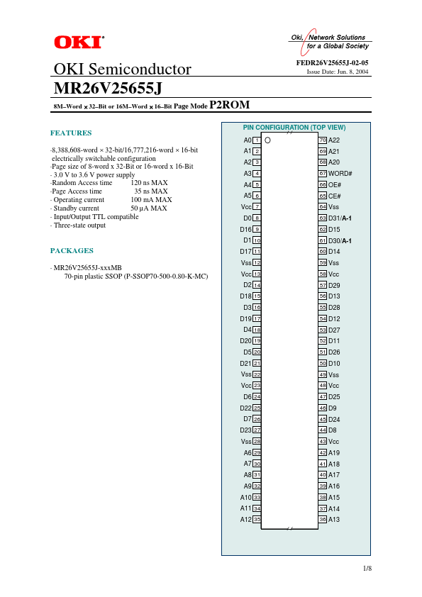
A1 2 A2 3 A3 4 A4 5 A5 6 Vcc 7 D0 8 D16 9 D1 10
PACKAGES
- MR26V25655J-xxx MB 70-pin plastic SSOP (P-SSOP70-500-0.80-K-MC)
D17 11 Vss 12 Vcc 13 D2 14 D18 15 D3 16 D19 17 D4 18 D20 19 D5 20 D21 21 Vss 22 Vcc 23 D6 24 D22 25 D7 26 D23 27 Vss 28 A6 29 A7 30 A8 31 A9 32 A10 33 A11 34 A12 35
1/8
FEDR26V25655J-02-05
OKI Semiconductor
MR26V25655J / P2ROM
BLOCK DIAGRAM
A- 1(D30/A-1[61] AND D31/A-1[63])
× 16/× 32 Switch CE# CE OE# OE WORD#
A0 A1 A2 A3 A4 A5 A6 A7 A8 A9 A10 A11 A12 A13 A14 A15 A16 A17 A18 A19 A20 A21 A22
Row Decoder
Memory Cell Matrix 8M × 32-Bit or 16M × 16-Bit
Address Buffer
Column Decoder
Multiplexer
Output Buffer
D0 D2 D4 D6 D8 D10 D12 D14 D16 D18 D20 D22 D24 D26 D28 D30 D1 D3 D5 D7 D9 D11 D13 D15 D17 D19 D21 D23 D25 D27 D29 D31 In16-bit output mode, these pins are placed in a high-Z state and pin D31,D30 functions as the A-1 address pin.
PIN DESCRIPTIONS
Pin name D31 / A- 1,D30/A-1 A0 to A22 D0 to D29 CE# OE# WORD# VCC VSS Address inputs Data outputs Chip enable input Output enable input Word -Byte select input Power supply voltage Ground Functions Data output / Address input
2/8
FEDR26V25655J-02-05
OKI Semiconductor
MR26V25655J / P2ROM
FUNCTION TABLE
Mode Read (32-Bit) Read (16Bit) Output disable Standby CE# L L L H OE# L L H ∗ WORD# H L H L H L 3.3 V DOUT VCC D0 to D15 D16 to D29 DOUT Hi- Z Hi- Z Hi- Z L/H ∗ ∗ D30/A- 1,D31/A-1
∗: Don’t Care (H or L)
ABSOLUTE MAXIMUM RATINGS
Parameter Operating temperature under bias Storage temperature Input voltage Output voltage Power supply voltage Power dissipation per package Symbol Ta Tstg VI VO VCC...