NJU7384
NJU7384 is Digital Signal Processor manufactured by New Japan Radio.
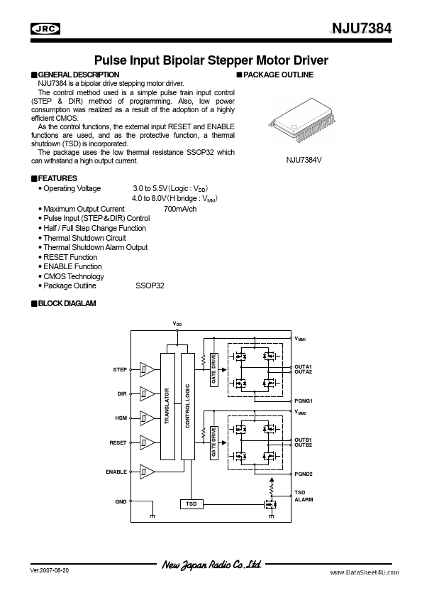
DESCRIPTION s PACKAGE OUTLINE NJU7384 is a bipolar drive stepping motor driver. The control method used is a simple pulse train input control (STEP & DIR) method of programming. Also, low power consumption was realized as a result of the adoption of a highly efficient CMOS. As the control functions, the external input RESET and ENABLE functions are used, and as the protective function, a thermal shutdown (TSD) is incorporated. The package uses the low thermal resistance SSOP32 which NJU7384V can withstand a high output current. s FEATURES
- Operating Voltage 3.0 to 5.5V(Logic : VDD) 4.0 to 8.0V(H bridge : VMM)
- Maximum Output Current 700m A/ch
- Pulse Input (STEP&DIR) Control
- Half / Full Step Change Function
- Thermal Shutdown Circuit
- Thermal Shutdown Alarm Output
- RESET Function
- ENABLE Function
- CMOS Technology
- Package Outline SSOP32 s BLOCK DIAGLAM
VDD VMM1
GATE DRIVE
STEP
OUTA1 OUTA2
CONTROL LOGIC
TRANSLATOR
PGNG1 VMM2
GATE DRIVE
RESET
OUTB1 OUTB2
ENABLE
PGND2
TSD ALARM
Ver.2007-08-20
-1-
NJU7384 s PIN FUNCTION
..
1 2 3 4 5 6 7 8 9 10 11 12 13 14 15 16
32 31 30 29 28 27 26 25 24 23 22 21 20 19 18 17
1. NC 2. NC 3. NC 4. VDD 5. NC 6. STEP 7. DIR 8. HSM 9. RESET 10. ENABLE 11. TSD ALARM 12. NC 13. GND 14. NC 15. NC 16. NC
32. VMM1 31. VMM1 30. OUTA1 29. OUTA1 28. OUTA2 27. OUTA2 26. PGND1 25. PGND1 24. PGND2 23. PGND2 22. OUTB2 21. OUTB2 20. OUTB1 19. OUTB1 18. VMM2 17. VMM2 s PIN DESCRIPTION
PIN No. 1,2,3 4 5 6 7 8 9 10 11 12 13 14,15,16 17,18 19,20 21,22 23,24 25,26 27,28 29,30 31,32 SYMBOL NC VDD NC STEP DIR HSM RESET ENABLE TSD ALARM NC GND NC VMM2 OUTB1 OUTB2 PGND2 PGND1 OUTA2 OUTA1 VMM1 FUNCTION Non connection pins Logic Power-Supply input pin Non connection pin Pulse signal input pin for motor rotation control pin Forward / Reverse rotation control Full / Half step mode control pin Phase initialize signal input pin NOTE 1 pulse input ⇒ 1 clock motion
“H”= Forward (CW), ”L”= Reverse (CCW) “H”= Full step,...