NJU6343
NJU6343 is 50MHz VCXO IC manufactured by New Japan Radio.
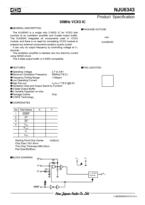
DESCRIPTION
The NJU6343 is a single chip C-MOS IC for VCXO that consists of an oscillation amplifier and 3-state output buffer. The NJU6343 integrates all ponents used in VCXO module, and there is no need for pleting VCXO module to prepare any external ponents except a quartz crystal. It can vary its output frequency by controlling voltage at VC terminal. The oscillation amplifier is realized very low stand-by current using NAND circuit. The 3-state output buffer is C-MOS patible. s FEATURES q Operating Voltage 2.7 to 3.6V q Maximum Oscillation Frequency 50MHz(T.B.D.) q Frequency Pulling Range ±100ppm q Low Operating Current q High Fan-out IOH/IOL= T.B.D @3.0V q Oscillation Stop and Output Stand-by Function q3-State Output Buffer q A Variable Capacitor on-chip q Package Outline Chip q C-MOS Technology s COORDINATES No 1 Pad Name X Y s PACKAGE OUTLINE
NJU6343C s PAD LOCATION
2 3 4
CONT XT
XT VSS FOUT VC VDD
Starting Point:Chip Center Unit[um] Chip Size:1.6x1.6mm Thin-Chip Thickness:260±20um Pad Size:90x90um s BLOCK DIAGRAM
Rf
Cg
Cd
- STATE BUFFER
FOUT
CONT
2002/03/11 ( 1 / 4 )
..
NJU6343 s TREMINAL DESCRIPTION
SYMBOL
CONT
FUNCTION Oscillation and 3-state Output Buffer Control FOUT CONT Frequency Output corresponding to Control H or OPEN Voltage. L Oscillation Stop and High impedance Output Quartz Crystal Connecting Terminals VSS=0V Frequency Output Frequency Control VDD=3.0V (Ta=25°C)
XT XT VSS FOUT VC VDD s ABSOLUTE MAXIMUM RATINGS
PARAMETER SYMBOL RATING UNIT Supply Voltage VDD -0.5 to +7.0 V Control Voltage VC VSS-0.5 to VDD+0.5 V Input Voltage VIN VSS-0.5 to VDD+0.5 V Output Voltage VO -0.5 to VDD+0.5 V m A Input Current IIN ±10 Output Current IO m A ±25 Operating Temperature Range Topr -40 to +85 °C Storage Temperature Range Tstg -55 to +125 °C Note1) If the supply voltage(VDD) is less than 7.0V, the input voltage must not over the VDD level though 7.0V is limit specified. Note2) Decupling capacitor should be connected between VDD and...