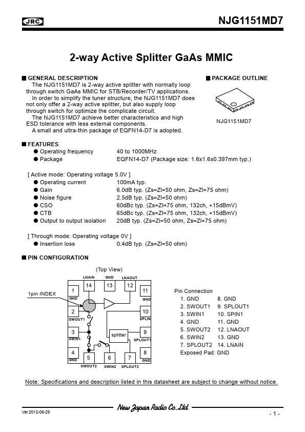
• Part: NJG1151MD7
  • Description: 2-way Active Splitter GaAs MMIC
  • Manufacturer: New Japan Radio
  • Size: 959.43 KB
Download NJG1151MD7 Datasheet PDF
New Japan Radio
NJG1151MD7
NJG1151MD7 is 2-way Active Splitter GaAs MMIC manufactured by New Japan Radio.
DESCRIPTION The NJG1151MD7 is 2-way active splitter with normally loop through switch Ga As MMIC for STB/Recorder/TV applications. In order to simplify the tuner structure, the NJG1151MD7 does not only offer a 2-way active splitter, but also supply loop through switch for optimize the plicate circuit. The NJG1151MD7 achieve better characteristics and high ESD tolerance with less external ponents. A small and ultra-thin package of EQFN14-D7 is adopted. I FEATURES G Operating frequency G Package [ Active mode: Operating voltage G Operating current G Gain G Noise figure G CSO G CTB G Output to output isolation I PACKAGE OUTLINE 40 to 1000MHz EQFN14-D7 (Package size: 1.6x1.6x0.397mm typ.) 5.0V ] 100m A typ. 6.0d B typ. (Zs=Zl=50 ohm, Zs=Zl=75 ohm) 2.5d B typ. (Zs=Zl=50 ohm) 60d Bc typ. (Zs=Zl=75 ohm, 132ch, +15d Bm V) 65d Bc typ. (Zs=Zl=75 ohm, 132ch, +15d Bm V) 20d B typ. (Zs=Zl=50 ohm, Zs=Zl=75 ohm) http://..net/ [ Through mode: Operating voltage 0V ] G Insertion loss 0.4d B typ. (Zs=Zl=50 ohm) I PIN CONFIGURATION (Top View) LNAIN GND LNAOUT 1pin INDEX 12 11 SWOUT1 SPLIN SWIN1 splitter splitter SPLOUT1 8 5 SWOUT2 Pin Connection 1. GND 2. SWOUT1 3. SWIN1 4. GND 5. SWOUT2 6. SWIN2 7. SPLOUT2 Exposed Pad: 8. GND 9. SPLOUT1 10. SPIN1 11. GND 12. LNAOUT 13. GND 14. LNAIN GND SWIN2 SPLOUT2 Note: Specifications and description listed in this datasheet are subject to change without notice. Ver.2012-06-29 -1datasheet pdf - http://..net/ I ABSOLUTE MAXIMUM RATINGS T a=+25°C, Zs=Zl=50 ohm / 75 ohm PARAMETER Drain voltage Input power Power dissipation Operating temperature Storage temperature SYMBOL VDD PIN PD Topr Tstg VDD=5.0V 4-layer FR4 PCB with through-hole (76.2x114.3mm), Tj=150°C CONDITIONS RATINGS 6.0 +10 1300 -40~+85 -55~+150 UNITS V d Bm m W °C °C I ELECTRICAL CHARACTERISTICS (DC CHARACTERISTICS) VDD=5.0V, T a=+25°C, with application circuit1 PARAMETERS SYMBOL VDD IDD RF OFF http://..net/ CONDITIONS...