Description
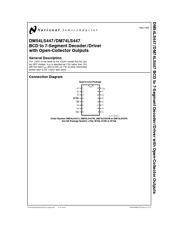
The ’LS447 is the same as the ’LS247 except that the Output OFF Voltage VOH is specified as 7 0V rather than 15V with the same IOH limit of 250 mA For all other information please refer to the ’LS247 data sheet Connection Diagram Dual-In-Line Package May 1992 TL F 10187 – 1 Order Number DM54LS447J DM54LS447W DM74LS447M or DM74LS447N See NS Package Number J16A M16A N16E or W16A C1995 National Semiconductor Corporation TL F 10187 RRD-B30M105 Printed in U S A If Military Aerospace specified devices are required please contact the National Semiconductor Sales Office Distributors for availability and specifications Supply Voltage 7V Input Voltage 7V Operating Free Air Temperature Range DM54LS b55 C to a125 C DM74LS 0 C to a70 C Storage Temperature Range b65 C to a150 C Note The ‘‘ Remended Operating Conditions Symbol Parameter VCC Supply Voltage VIH High Level Input Voltage VIL Low Level Input Voltage IOH High Level Output Current (BI RBO) IOL Low Level Output Current TA Free Air Operating Temperature DM54LS447 Min Nom Max 45 5 55 2 07 b50 12 b55 125 DM74LS447 Min Nom Max 4 75 5 5 25 2 08 b50 24 0 70 Units V V V mA mA C Symbol Parameter Conditions Min VI Input Clamp Voltage VCC e Min II e b18 mA VOH High Level Output VCC e Min IOH e Max DM54 24 Voltage VIL e Max (BI RBO) DM74 24 IOFF VOL High Level Output Current Low Level Output Voltage Segment Outputs VO e 7 0V (a – g) VCC Min IOL e Max VIH e Min DM54 DM74 IOL e 12 mA VCC e Min DM74 II Input Current Max VCC e Max VI e 7V Input Voltage VI e 10V (DM54) IIH High Level Input Current VCC e Max VI e 2 7V IIL Low Level Input Current VCC e Max VI e 0 4V Others BI RBO Inputs IOS Short Circuit Output Current VCC e Max (Note 2) DM54 DM74 b0 3 b0 3 ICC Supply Current VCC e Max Note 1 All typicals are at VCC e 5V TA e 25 C Note 2 Not more than one output should be shorted at a time and the duration should not exceed one second Typ (Note 1) 34 0 35 0 25 Max b1 5 250 04 05 04 01 20 b0 4 b1 2 b2 0 b2 0 13 Units V V mA V mA mA mA mA mA mA Switching Characteristics at VCC e 5V TA e 25 C Symbol Parameter RL e 2 kX CL e 15 pF Min Max tPLH Propagation Delay 100 tPHL 100 Units ns 2 Logic Symbol State Diagram VCC e Pin 16 GND e Pin 8 TL F 10187–2 TL F 10187 – 3 3 Physical Dimensions inches (millimeters) 16-Lead Ceramic Dual-In-Line Package (J) Order Number DM54LS447J NS Package Number J16A 4 Physical Dimensions inches (millimeters) (Continued) 16-Lead Small Outline Molded Package (M) Order Number DM74LS447M NS Package Number M16A 16-Lead Molded Dual-In-Line Package (N) Order Number DM74LS447N NS Package Number N16E 5 DM54LS447 DM74LS447 BCD to 7-Segment Decoder Driver with Open-Collector Outputs Physical Dimensions inches (millimeters) (Continued) 16-Lead Ceramic Flat Package (W) Order Number DM54LS447W NS Package Number W16A LIFE SUPPORT POLICY NATIONAL’S PRODUCTS ARE NOT AUTHORIZED FOR USE AS CRITICAL PONENTS IN LIFE SUPPORT DEVICES OR SYSTEMS WITHOUT THE EXPRESS WRITTEN APPROVAL OF THE PRESIDENT OF NATIONAL SEMICONDUCTOR CORPORATION As used herein 1 Life support devices or systems are devices or systems which (a) are intended for surgical implant into the body or (b) suppor.