Datasheet4U Logo Datasheet4U.com

DM54LS367A - Hex TRI-STATE Buffers

Download the DM54LS367A datasheet PDF. This datasheet also covers the DM54LS367AJ variant, as both devices belong to the same hex tri-state buffers family and are provided as variant models within a single manufacturer datasheet.
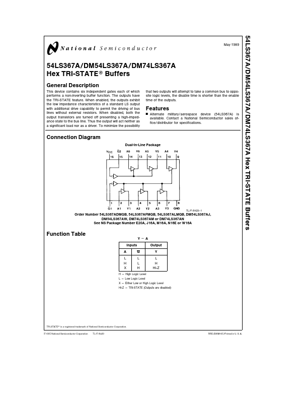
Description

This device contains six independent gates each of which performs a non-inverting buffer function The outputs have the TRI-STATE feature When enabled the outputs exhibit the low impedance characteristics of a standard LS output with additional drive capability to permit the driving of bus lines with

Features

  • Y Alternate military aerospace device (54LS367A) is available Contact a National Semiconductor sales office distributor for specifications Connection Diagram Dual-In-Line Package TL F 6429.
  • 1 Order Number 54LS367ADMQB 54LS367AFMQB 54LS367ALMQB DM54LS367AJ DM54LS367AW DM74LS367AM or DM74LS367AN See NS Package Number E20A J16A M16A N16E or W16A Function Table YeA Inputs Output AG Y LL HL XH L H Hi-Z H e High Logic Level L e Low Logic Level X e Either Low or High Logic Level Hi.

📥 Download Datasheet

Note: The manufacturer provides a single datasheet file (DM54LS367AJ_NationalSemiconductor.pdf) that lists specifications for multiple related part numbers.

Full PDF Text Transcription (Reference)

The following content is an automatically extracted verbatim text from the original manufacturer datasheet and is provided for reference purposes only.

View original datasheet text
54LS367A DM54LS367A DM74LS367A Hex TRI-STATE Buffers May 1989 54LS367A DM54LS367A DM74LS367A Hex TRI-STATE Buffers General Description This device contains six independent gates each of which performs a non-inverting buffer function The outputs have the TRI-STATE feature When enabled the outputs exhibit the low impedance characteristics of a standard LS output with additional drive capability to permit the driving of bus lines without external resistors When disabled both the output transistors are turned off presenting a high-impedance state to the bus line Thus the output will act neither as a significant load nor as a driver To minimize the possibility that two outputs will attempt to take a common bus to opposite logic levels the disable time is shorter than the enable time of the
Published: |