CGS74C2525
CGS74C2525 is 1-to-8 Minimum Skew Clock Driver manufactured by National Semiconductor.
CGS74C2525 CGS74CT2525 CGS74C2526 CGS74CT2526 1-to-8 Minimum Skew Clock Driver
September 1995
CGS74C2525 CGS74CT2525 CGS74C2526 CGS74CT2526 1-to-8 Minimum Skew Clock Driver
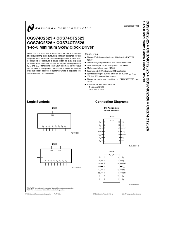
The CGS ’C CT2525 is a minimum skew clock driver with one input driving eight outputs specifically designed for signal generation and clock distribution applications The ’2525 is designed to distribute a single clock to eight separate receivers with low skew across all outputs during both the t PLH and t PHL transitions The ’2526 is similar to the ’2525 but contains a multiplexed clock input to allow for systems with dual clock speeds or systems where a separate test clock has been implemented
Features
Y Y Y Y Y Y Y Y
These CGS devices implement National’s FACTTM family Ideal for signal generation and clock distribution Guaranteed pin to pin and part to part skew Multiplexed clock input (’2526) Guaranteed 2 k V minimum ESD protection Symmetric output current drive of 24 m A for IOL IOH ’CT has TTL-patible inputs These products are identical to 74AC ACT2525 and 2526 Available as Mil Aero versions 54AC ACT2525 54AC ACT2526
Logic Symbols
’2525
Connection Diagrams
Pin Assignment for DIP and SOIC ’2525
TL F 10684
- 1
’2526
TL F 10684
- 3
’2526
TL F 10684
- 2
TL F 10684
- 4
TRI-STATE is a registered trademark of National Semiconductor Corporation FACTTM is a trademark of National Semiconductor Corporation C1996 National Semiconductor Corporation TL F 10684 RRD-B30M106 Printed in U S A http
national
Functional Description
On the multiplexed clock device the SEL pin is used to determine which CLKn input will have an active effect on the outputs of the circuit When SEL e 1 the CLK1 input is selected and when SEL e 0 the CLK0 input is selected The non-selected CLKn input will not have any effect on the logical output level of the circuit The output pins act as a single entity and will follow the state of the CLK or CLK1 CLK0 pins when either the multiplexed (’2526) or...