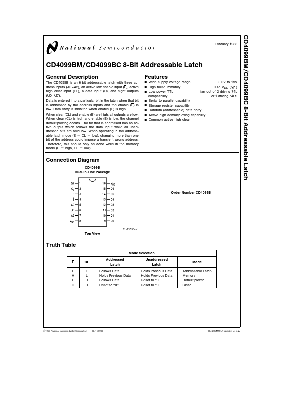
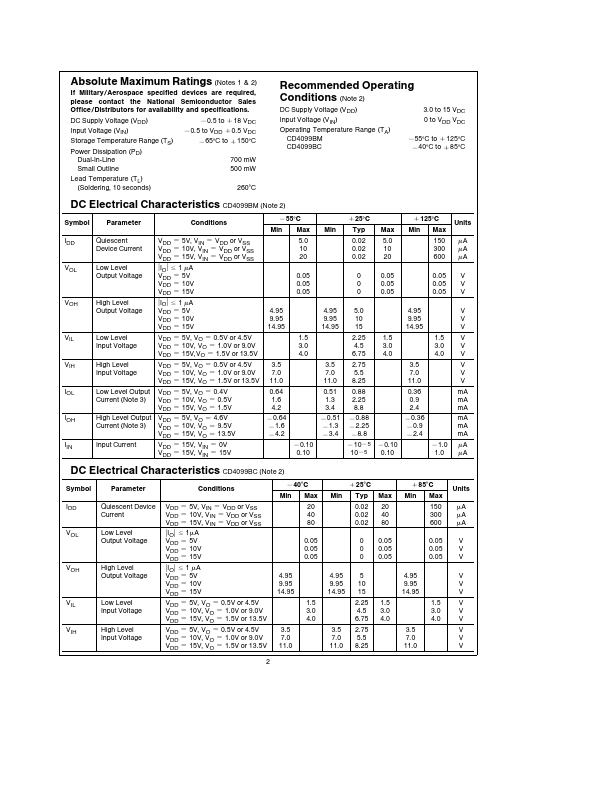
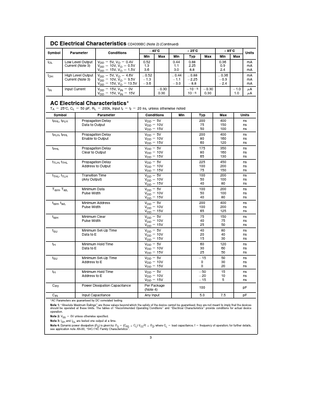
Datasheet4U Logo Datasheet4U.com

CD4099BC - 8-Bit Addressable Latch

Datasheet Summary

Description

The CD4099B is an 8-bit addressable latch with three address inputs (A0 A2) an active low enable input (E) active high clear input (CL) a data input (D) and eight outputs (Q0 Q7) Data is entered into a particular bit in the latch when that bit is addressed by the address inputs and

Features

  • Y Y Y Y Y Y Y Y Wide supply voltage range 3 0V to 15V High noise immunity 0 45 VDD (typ ) Low power TTL fan out of 2 driving 74L compatibility or 1 driving 74LS Serial to parallel capability Storage register capability Random (addressable) data entry Active high demultiplexing capability Common active high clear Connection Diagram CD4099B Dual-In-Line Package Order Number CD4099B TL F 5984.
  • 1 Top View Truth Table Mode Selection E L H L H CL L L H H Addressed Latch Follows Data Ho.

📥 Download Datasheet

Datasheet preview – CD4099BC
Other Datasheets by National Semiconductor

Full PDF Text Transcription

Click to expand full text
CD4099BM CD4099BC 8-Bit Addressable Latch February 1988 CD4099BM CD4099BC 8-Bit Addressable Latch General Description The CD4099B is an 8-bit addressable latch with three address inputs (A0–A2) an active low enable input (E) active high clear input (CL) a data input (D) and eight outputs (Q0 – Q7) Data is entered into a particular bit in the latch when that bit is addressed by the address inputs and the enable (E) is low Data entry is inhibited when enable (E) is high When clear (CL) and enable (E) are high all outputs are low When clear (CL) is high and enable (E) is low the channel demultiplexing occurs The bit that is addressed has an active output which follows the data input while all unaddressed bits are held low When operating in the addressable latch mode (E e CL e low) changing
Published: |