Datasheet Summary
CD4093BM CD4093BC Quad 2-Input NAND Schmitt Trigger
February 1993
CD4093BM CD4093BC Quad 2-Input NAND Schmitt Trigger
General Description
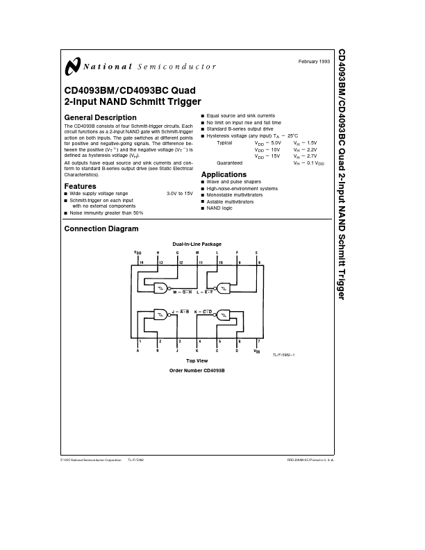
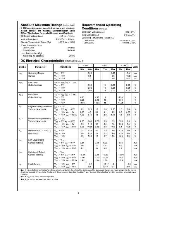
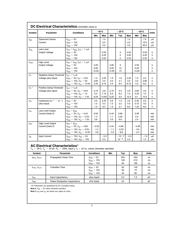
The CD4093B consists of four Schmitt-trigger circuits Each circuit functions as a 2-input NAND gate with Schmitt-trigger action on both inputs The gate switches at different points for positive and negative-going signals The difference between the positive (VT a ) and the negative voltage (VTb) is defined as hysteresis voltage (VH) All outputs have equal source and sink currents and conform to standard B-series output drive (see Static Electrical Characteristics)
Equal source and sink currents No limit on input rise and fall time Standard...