CD4042BM
Description
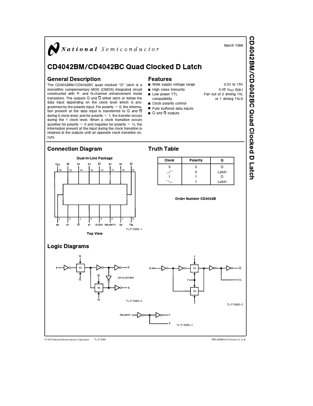
The CD4042BM CD4042BC quad clocked ‘‘D’’ latch is a monolithic plementary MOS (CMOS) integrated circuit constructed with P- and N-channel enhancement mode transistors The outputs Q and Q either latch or follow the data input depending on the clock level which is programmed by the polarity input For polarity e 0 the information present at the data input is transferred to Q and Q during 0 clock level and for polarity e 1 the transfer occurs during the 1 clock level When a clock transition occurs (positive for polarity e 0 and negative for polarity e 1) the information present at the input during the clock transition is retained at the outputs until an opposite clock transition occurs
Features
Wide supply voltage range High noise immunity Low power TTL patibility Clock polarity control Fully buffered data inputs Q and Q outputs
3 0V to 15V 0 45 VDD (typ ) Fan out of 2 driving 74L or 1 driving 74LS
Connection Diagram
Dual-In-Line Package
Truth Table
Clock 0 L...