Datasheet Summary
CD4041UB CD4041UBC Quad True plement Buffer
February 1988
CD4041UB CD4041UBC Quad True plement Buffer
General Description
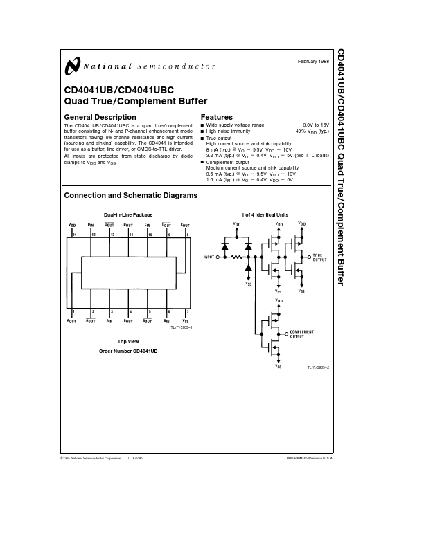
The CD4041UB CD4041UBC is a quad true plement buffer consisting of N- and P-channel enhancement mode transistors having low-channel resistance and high current (sourcing and sinking) capability The CD4041 is intended for use as a buffer line driver or CMOS-to-TTL driver All inputs are protected from static discharge by diode clamps to VDD and VSS
Features
Wide supply voltage range 3 0V to 15V High noise immunity 40% VDD (typ ) True output High current source and sink capability 8 mA (typ ) VO e 9 5V VDD e 10V 3 2 mA (typ ) VO e 0 4V VDD e 5V (two...