CD4035BC Overview
Key Specifications
Package: DIP
Operating Voltage: 5 V
Max Voltage (typical range): 15 V
Min Voltage (typical range): 3 V
Description
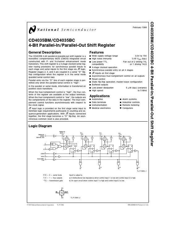
The CD4035B 4-bit parallel-in parallel-out shift register is a monolithic complementary MOS (CMOS) integrated circuit constructed with P- and N-channel enhancement mode transistors This shift register is a 4-stage clocked serial register having provisions for synchronous parallel inputs to each stage and serial inputs to the first stage via JK logic Register stages 2 3 and 4 are coupled in a serial ‘‘D’’ flipflop configuration when the register is in the serial mode (parallel serial control low) Parallel entry via the ‘‘D’’ line of each register stage is permitted only when the parallel serial control is ‘‘high’’ In the parallel or serial mode information is transferred on positive clock transitions When the true complement control is ‘‘high’’ the true contents of the register are available at the output terminals When the true complement control is ‘‘low’’ the outputs are the complements of the data in the register The true complement control functions asynchronously with respect to the clock signal JK input logic is provided on the first stage serial input to minimize logic requirements particularly in counting and sequence-generation applications With JK inputs connected together the first stage becomes a ‘‘D’’ flip-flop An asynchronous common reset is also provided.