CD4025C Overview
Key Specifications
Package: DIP
Operating Voltage: 5 V
Max Voltage (typical range): 15 V
Min Voltage (typical range): 3 V
Description
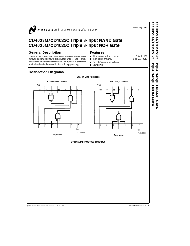
These triple gates are monolithic complementary MOS (CMOS) integrated circuits constructed with N- and P-channel enhancement mode transistors All inputs are protected against static discharge with diodes to VDD and VSS.