CD40174BM
CD40174BM is Hex/Quad D Flip-Flop manufactured by National Semiconductor.
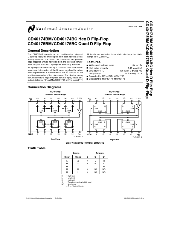
CD40174BM CD40174BC Hex D Flip-Flop CD40175BM CD40175BC Quad D Flip-Flop
February 1988
CD40174BM CD40174BC Hex D Flip-Flop CD40175BM CD40175BC Quad D Flip-Flop
General Description
The CD40174B consists of six positive-edge triggered D-type flip-flops the true outputs from each flip-flop are externally available The CD40175B consists of four positiveedge triggered D-type flip-flops both the true and plement outputs from each flip-flop are externally available All flip-flops are controlled by a mon clock and a mon clear Information at the D inputs meeting the set-up time requirements is transferred to the Q outputs on the positive-going edge of the clock pulse The clearing...