CD4006BM
Overview
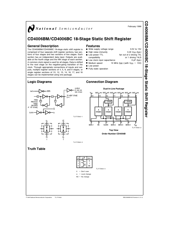
The CD4006BM CD4006BC 18-stage static shift register is comprised of four separate shift register sections two sections of four stages and two sections of five stages Each section has an independent data input Outputs are available at the fourth stage and the fifth stage of each section A common clock signal is used for all stages Data is shifted to the next stage on the negative-going transition of the clock Through appropriate connections of inputs and outputs multiple register sections of 4 5 8 and 9 stages or single register sections of 10 12 13 14 16 17 and 18 stages can be implemented using one package.