Description
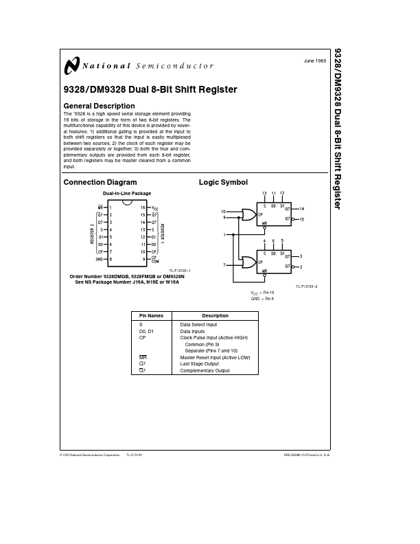
The ’9328 is a high speed serial storage element providing 16 bits of storage in the form of two 8-bit registers The multifunctional capability of this device is provided by several features 1) additional gating is provided at the input to both shift registers so that the input is easily multiplexed between two sources 2) the clock of each register may be provided separately or together 3) both the true and complementary outputs are provided from each 8-bit register and both registers may be master cleared from a common input Connection Diagram Dual-In-Line Package Logic Symbol TL F 9793 - 1 Order Number 9328DMQB 9328FMQB or DM9328N See NS Package Number J16A N16E or W16A TL F 9793 - 2 VCC e Pin 16 GND e Pin 8 Pin Names S D0 D1 CP Description Data Select Input Data Inputs Clock Pulse Input (Active HIGH) Common (Pin 9) Separate (Pins 7 and 10) Master Reset Input (Active LOW) Last Stage Output Complementary Output MR Q7 Q7 C1995 National Semiconductor Corporation TL F 9793 RRD-B30M115 Printed in U S A.