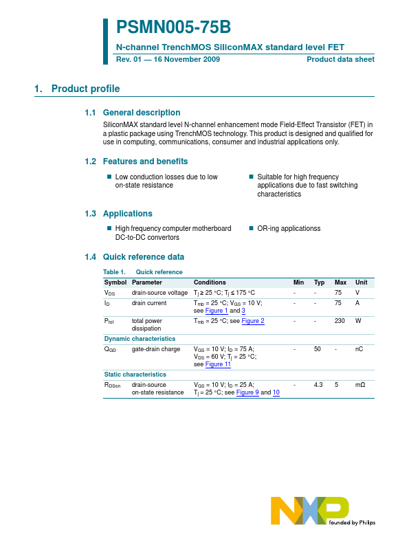
PSMN005-75B
PSMN005-75B is N-Channel MOSFET manufactured by NXP Semiconductors.
description
Silicon MAX standard level N-channel enhancement mode Field-Effect Transistor (FET) in a plastic package using Trench MOS technology. This product is designed and qualified for use in puting, munications, consumer and industrial applications only.
1.2 Features and benefits
- Low conduction losses due to low on-state resistance
- Suitable for high frequency applications due to fast switching characteristics
1.3 Applications
- High frequency puter motherboard DC-to-DC convertors
- OR-ing applicationss
1.4 Quick reference data
Table 1. VDS ID Ptot Quick reference Conditions Tmb = 25 °C; VGS = 10 V; see Figure 1 and 3 Tmb = 25 °C; see Figure 2 Min Typ Max 75 75 230 Unit V A W drain-source voltage Tj ≥ 25 °C; Tj ≤ 175 °C drain current total power dissipation gate-drain charge Symbol Parameter
Dynamic characteristics QGD VGS = 10 V; ID = 75 A; VDS = 60 V; Tj = 25 °C; see Figure 11 VGS = 10 V; ID = 25 A; Tj = 25 °C; see Figure 9 and 10 50 n C
Static characteristics RDSon drain-source on-state resistance 4.3 5 mΩ
NXP Semiconductors
N-channel Trench MOS Silicon MAX standard level FET
2. Pinning information
Table 2. Pin 1 2 3 mb Pinning information Symbol G D S D Description gate drain source drain mbb076
Simplified outline
[1]
Graphic symbol
D mb
2 1 3
SOT404 (D2PAK)
[1] It is not possible to make connection to pin 2.
3. Ordering information
Table 3. Ordering information Package Name PSMN005-75B D2PAK Description plastic single-ended surface-mounted package (D2PAK); 3 leads (one lead cropped) Version SOT404 Type number
PSMN005-75B_1
© NXP B.V. 2009. All rights reserved.
Product data sheet
Rev. 01
- 16 November 2009
2 of 13
NXP Semiconductors
N-channel Trench MOS Silicon MAX standard level FET
4. Limiting values
Table 4. Symbol VDS VDGR VGS ID IDM Ptot Tstg Tj VGSM Limiting values Parameter drain-source voltage drain-gate voltage gate-source voltage drain current peak drain current total power dissipation storage...