Download PHX3055E Datasheet PDF
NXP Semiconductors
PHX3055E
FEATURES - ’Trench’ technology - Low on-state resistance - Fast switching - Isolated mounting tab SYMBOL d QUICK REFERENCE DATA VDSS = 55 V ID = 9 A g RDS(ON) ≤ 150 mΩ (VGS = 10 V) s GENERAL DESCRIPTION 
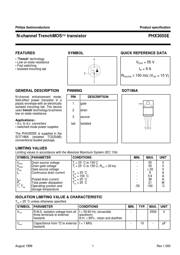
N-channel enhancement mode, field-effect power transistor in a plastic envelope with an electrically isolated mounting tab. The device uses ’trench’ technology to achieve low on-state resistance. Applications:- d.c. to d.c. converters - switched mode power supplies The PHX3055E is supplied in the SOT186A (isolated TO220AB) conventional leaded package. PINNING PIN 1 2 3 tab gate drain source isolated DESCRIPTION SOT186A case 1 2 3 LIMITING VALUES Limiting values in accordance with the Absolute Maximum System (IEC 134) SYMBOL PARAMETER VDSS VDGR VGS ID IDM PD Tj, Tstg Drain-source voltage Drain-gate voltage Gate-source voltage Continuous drain current Pulsed drain current Total power dissipation Operating junction and storage temperature CONDITIONS Tj = 25 ˚C to 150˚C Tj = 25 ˚C...