PHX2N40E
Overview
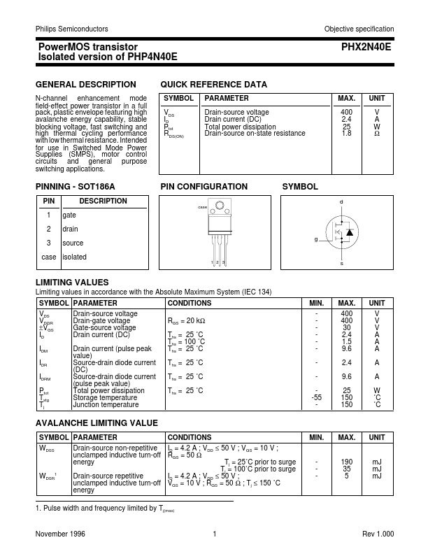
Philips Semiconductors Objective specification PowerMOS transistor Isolated version of PHP4N40E GENERAL DESCRIPTION N-channel enhancement mode field-effect power transistor in a full pack, plastic e...
| Part | PHX2N40E |
|---|---|
| Description | PowerMOS transistor Isolated version of PHP4N40E |
| Category | Transistor |
| Manufacturer | NXP Semiconductors |
| Size | 24.90 KB |
Philips Semiconductors Objective specification PowerMOS transistor Isolated version of PHP4N40E GENERAL DESCRIPTION N-channel enhancement mode field-effect power transistor in a full pack, plastic e...
| Part Number | Manufacturer | Description |
|---|---|---|
| PHP4N40E | NXP Semiconductors | PowerMOS transistors Avalanche energy rated |