• Part: PHP96NQ03LT
  • Description: N-channel enhancement mode field-effect transistor
  • Category: Transistor
  • Manufacturer: NXP Semiconductors
  • Size: 293.21 KB
Download PHP96NQ03LT Datasheet PDF
NXP Semiconductors
PHP96NQ03LT
PHP96NQ03LT is N-channel enhancement mode field-effect transistor manufactured by NXP Semiconductors.
Description 
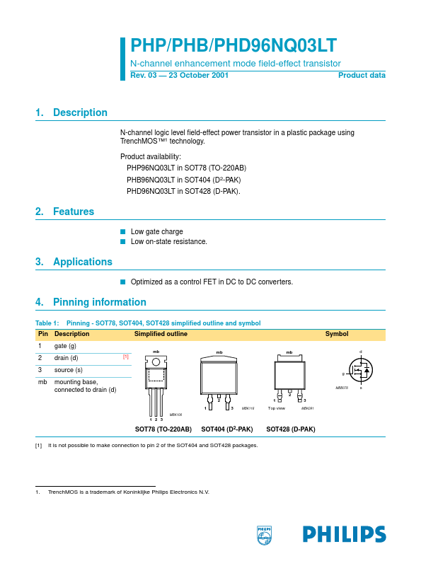
N-channel logic level field-effect power transistor in a plastic package using Trench MOS™1 technology. Product availability: PHP96NQ03LT in SOT78 (TO-220AB) PHB96NQ03LT in SOT404 (D2-PAK) PHD96NQ03LT in SOT428 (D-PAK). 2. Features s Low gate charge s Low on-state resistance. 3. Applications s Optimized as a control FET in DC to DC converters. 4. Pinning information Table 1: Pinning - SOT78, SOT404, SOT428 simplified outline and symbol Simplified outline mb mb mb Pin Description 1 2 3 mb gate (g) Symbol d drain (d) source (s) mounting base, connected to drain (d) [1] g s MBB076 2 2 1 MBK106 1 3 MBK116 MBK091 Top view 1 2 3 SOT78 (TO-220AB) [1] SOT404 (D2-PAK) SOT428 (D-PAK) It is not possible to make connection to pin 2 of the SOT404 and SOT428 packages. 1. Trench MOS is a trademark of Koninklijke Philips Electronics N.V. Philips Semiconductors PHP/PHB/PHD96NQ03LT N-channel enhancement mode field-effect transistor 5. Quick reference data Table 2: VDS ID Ptot Tj RDSon Quick reference data Conditions Tj = 25 to 175 °C Tmb = 25 °C; VGS = 5 V Tmb = 25 °C Tj = 25° C; VGS = 10 V; ID = 25 A Tj = 25° C; VGS = 5 V; ID = 25 A Typ 4.2 5.6 Max 25 75 115 175 4.95 7.5 Unit V A W °C mΩ mΩ drain-source voltage (DC) drain current (DC) total power dissipation junction temperature drain-source on-state resistance Symbol Parameter 6. Limiting values Table 3: Limiting values In accordance with the Absolute Maximum Rating System (IEC 60134). Symbol Parameter VDS VDGR VGS VGSM ID IDM Ptot Tstg Tj IS ISM drain-source voltage (DC) drain-gate voltage (DC) gate-source voltage (DC) gate-source voltage drain current (DC) peak drain current total power dissipation storage temperature operating junction temperature source (diode forward) current (DC) Tmb = 25 °C peak source (diode forward) current Tmb = 25 °C; pulsed; tp ≤ 10 µs tp ≤ 50 µs; pulsed; duty cycle 25%; Tj ≤ 150 °C Tmb = 25 °C; VGS = 5 V; Figure 2 and 3 Tmb = 100 °C; VGS = 5 V; Figure 2 Tmb = 25 °C;...