Download PHP3N20L Datasheet PDF
NXP Semiconductors
PHP3N20L
PHP3N20L is PowerMOS transistor Logic level FET manufactured by NXP Semiconductors.
Philips Semiconductors Product specification Power MOS transistor Logic level FET GENERAL DESCRIPTION 
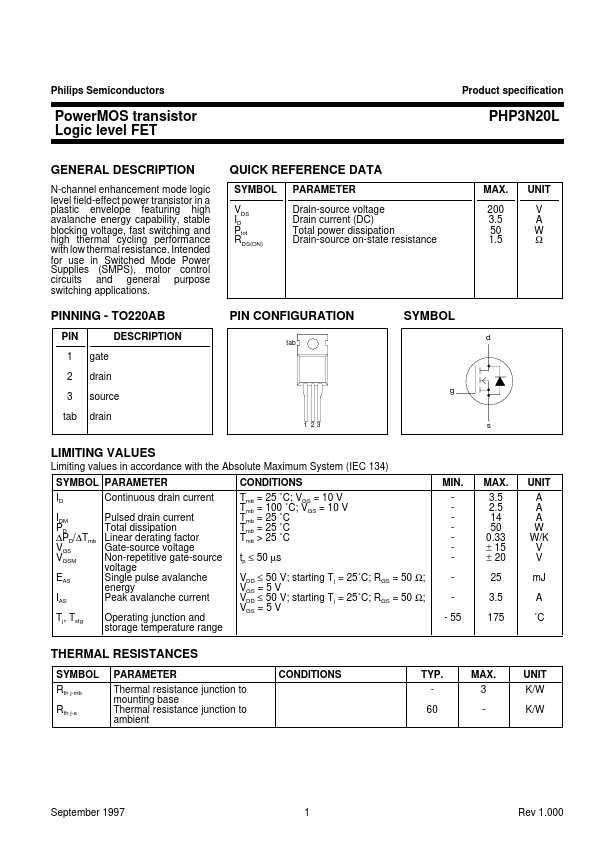
N-channel enhancement mode logic level field-effect power transistor in a plastic envelope featuring high avalanche energy capability, stable blocking voltage, fast switching and high thermal cycling performance with low thermal resistance. Intended for use in Switched Mode Power Supplies (SMPS), motor control circuits and general purpose switching applications. QUICK REFERENCE DATA SYMBOL VDS ID Ptot RDS(ON) PARAMETER Drain-source voltage Drain current (DC) Total power dissipation Drain-source on-state resistance MAX. 200 3.5 50 1.5 UNIT V A W Ω PINNING - TO220AB PIN 1 2 3 tab gate drain source drain DESCRIPTION PIN CONFIGURATION tab SYMBOL d g 1 23 s LIMITING VALUES Limiting values in accordance with the Absolute Maximum System (IEC 134) SYMBOL PARAMETER ID IDM PD ∆PD/∆Tmb VGS VGSM EAS IAS Tj, Tstg Continuous drain current Pulsed drain current Total dissipation Linear derating factor Gate-source voltage Non-repetitive gate-source voltage Single pulse avalanche energy Peak avalanche current Operating junction and storage temperature range CONDITIONS Tmb = 25 ˚C; VGS = 10 V Tmb = 100 ˚C; VGS = 10 V Tmb = 25 ˚C Tmb = 25 ˚C Tmb > 25 ˚C tp ≤ 50 µs VDD ≤ 50 V; starting Tj = 25˚C; RGS = 50 Ω; VGS = 5 V VDD ≤ 50 V; starting Tj = 25˚C; RGS = 50 Ω; VGS = 5 V MIN. - 55 MAX. 3.5 2.5 14 50 0.33 ± 15 ± 20 25 3.5 175 UNIT A A A W W/K V V m J A ˚C THERMAL RESISTANCES SYMBOL Rth j-mb Rth j-a PARAMETER Thermal resistance junction to mounting base Thermal resistance junction to ambient CONDITIONS TYP. 60 MAX. 3 UNIT K/W K/W September 1997 Rev 1.000 Philips Semiconductors Product specification Power MOS transistor Logic level FET ELECTRICAL CHARACTERISTICS Tj = 25 ˚C unless otherwise specified SYMBOL V(BR)DSS ∆V(BR)DSS / ∆Tj RDS(ON) VGS(TO) gfs IDSS IGSS Qg(tot) Qgs Qgd td(on) tr td(off) tf Ld Ld Ls Ciss Coss Crss PARAMETER Drain-source breakdown voltage...