Datasheet Summary
PHP20N06T; PHB20N06T
N-channel TrenchMOS™ transistor
Rev. 01
- 22 February 2001 Product specification
1. Description
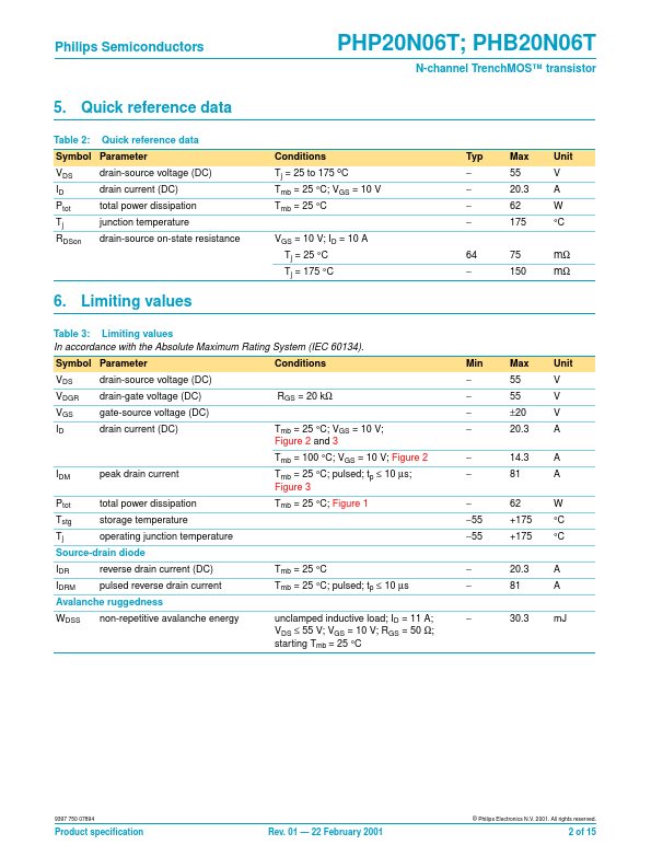
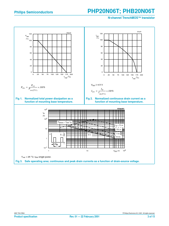
N-channel enhancement mode field-effect transistor in a plastic package using TrenchMOS™1 technology. Product availability: PHP20N06T in SOT78 (TO-220AB) PHB20N06T in SOT404 (D 2-PAK).
2. Features s Very low on-state resistance s Fast switching.
3. Applications s Switched mode power supplies s DC to DC converters. c
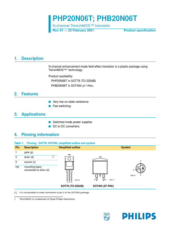
4. Pinning information c
Table 1: Pin 1 2 3 mb
Pinning
- SOT78, SOT404, simplified outline and symbol Description gate (g) mb
Simplified outline
Symbol drain (d) source (s) mounting base; connected to drain (d)
[1] mb d g s
MBK106
MBB076
MBK116...