PHF9NQ20 Overview
Description
N-channel, enhancement mode field-effect power transistor using Trench technology, intended for use in off-line switched mode power supplies, T.V. and computer monitor power supplies, d.c.
Key Features
- Low on-state resistance
- Fast switching
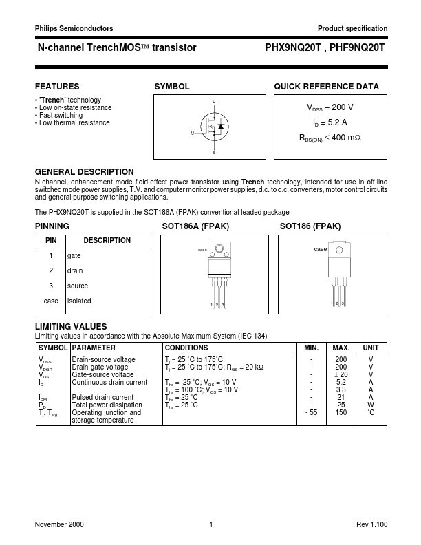
- Low SYMBOL d QUICK REFERENCE DATA VDSS = 200 V ID = 5.2 A g RDS(ON) ≤ 400 mΩ s