PHD6N10E Overview
Description
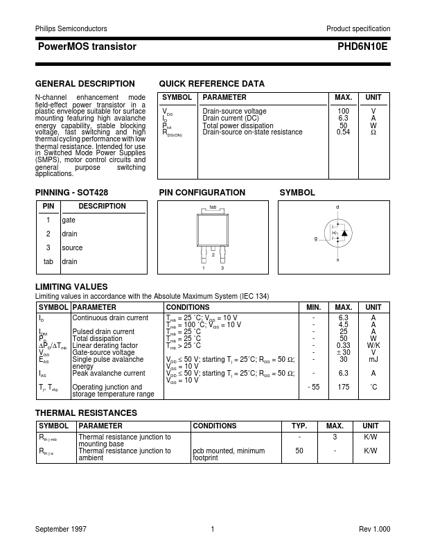
N-channel enhancement mode field-effect power transistor in a plastic envelope suitable for surface mounting featuring high avalanche energy capability, stable blocking voltage, fast switching and high thermal cycling performance with low QUICK REFERENCE DATA SYMBOL VDS ID Ptot RDS(ON) PARAMETER Drain-source voltage Drain current (DC) Total power dissipation Drain-source on-state resistance MAX. 100 6.3 50 0.54 UNIT V A W Ω PINNING - SOT428 PIN 1 2 3 tab gate drain source DESCRIPTION.