• Part: PHB130N03T
  • Description: TrenchMOS transistor Standard level FET
  • Category: Transistor
  • Manufacturer: NXP Semiconductors
  • Size: 65.45 KB
Download PHB130N03T Datasheet PDF
NXP Semiconductors
PHB130N03T
PHB130N03T is TrenchMOS transistor Standard level FET manufactured by NXP Semiconductors.
DESCRIPTION N-channel enhancement mode standard level field-effect power transistor in a plastic envelope suitable for surface mounting using ’trench’ technology. The device features very low on-state resistance and has integral zener diodes giving ESD protection up to 2k V. It is intended for use in DC-DC converters and general purpose switching applications. QUICK REFERENCE DATA SYMBOL VDS ID Ptot Tj RDS(ON) PARAMETER Drain-source voltage Drain current (DC)1 Total power dissipation Junction temperature Drain-source on-state resistance VGS = 10 V MAX. 30 75 188 175 6 UNIT V A W ˚C mΩ PINNING - SOT404 PIN 1 2 3 mb gate drain source drain DESCRIPTION PIN CONFIGURATION mb SYMBOL d g 2 1 3 s LIMITING VALUES Limiting values in accordance with the Absolute Maximum System (IEC 134) SYMBOL VDS VDGR ±VGS ID ID IDM Ptot Tstg, Tj PARAMETER Drain-source voltage Drain-gate voltage Gate-source voltage Drain current (DC)1 Drain current (DC)1 Drain current (pulse peak value) Total power dissipation Storage & operating temperature CONDITIONS RGS = 20 kΩ Tmb = 25 ˚C Tmb = 100 ˚C Tmb = 25 ˚C Tmb = 25 ˚C MIN. - 55 MAX. 30 30 20 75 75 240 188 175 UNIT V V V A A A W ˚C THERMAL RESISTANCES SYMBOL Rth j-mb Rth j-a PARAMETER Thermal resistance junction to mounting base Thermal resistance junction to ambient CONDITIONS minimum footprint, FR4 board TYP. 50 MAX. 0.8 UNIT K/W K/W 1 Current limited by package to 75A from a theoretical value of 130A. December 1997 1 Rev 1.200 
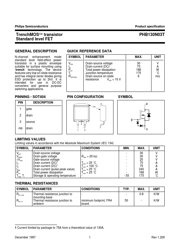
Philips Semiconductors Product specification Trench MOS™ transistor Standard level FET ESD LIMITING VALUE SYMBOL VC PARAMETER Electrostatic discharge capacitor voltage, all pins CONDITIONS Human body model (100 p F, 1.5 kΩ) MIN. - PHB130N03T MAX. 2 UNIT k V STATIC CHARACTERISTICS Tj= 25˚C unless otherwise specified SYMBOL V(BR)DSS VGS(TO) IDSS IGSS ±V(BR)GSS RDS(ON) PARAMETER Drain-source breakdown voltage Gate threshold voltage Zero gate voltage drain current Gate source leakage current Gate-source...