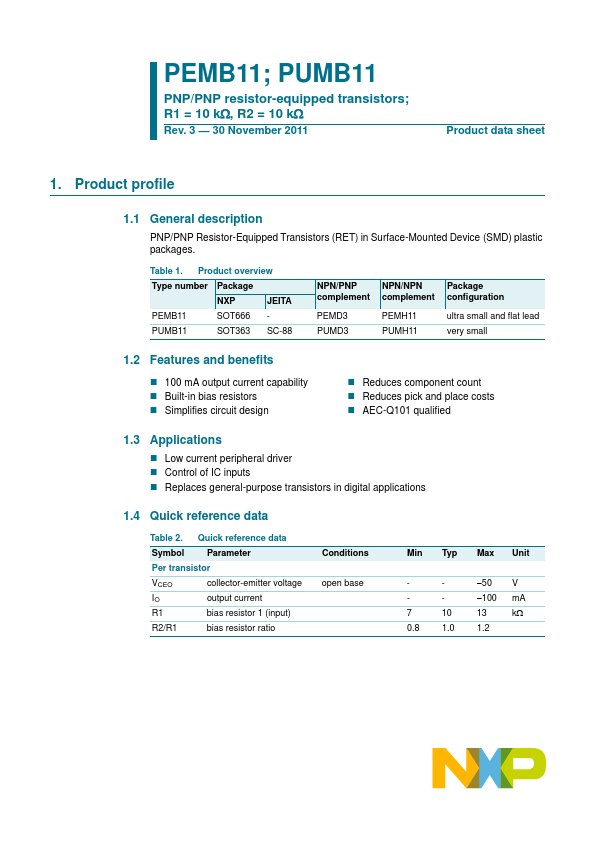
PEMB11
FEATURES
- 300 m W total power dissipation
- Very small 1.6 mm x 1.2 mm ultra thin package
- Excellent coplanarity due to straight leads
- Replaces two SC-75/SC-89 packaged transistors on same PCB area
- Reduces required PCB area
- Reduced pick and place costs. APPLICATIONS
- General purpose switching and amplification
- Inverter and interface circuits
- Circuit driver. DESCRIPTION
PNP resistor-equipped transistors in a SOT666 plastic package. MARKING TYPE NUMBER PEMB11 MARKING CODE B1
Top view TR1 6
QUICK REFERENCE DATA SYMBOL VCEO ICM TR1 TR2 R1 R2 PINNING PIN 1, 4 2, 5 6, 3 emitter base collector DESCRIPTION
TR1; TR2 TR1; TR2 TR1; TR2 PARAMETER collector-emitter voltage peak collector current PNP PNP bias resistor bias resistor MAX.
- 50
- 100
- - 10 10 UNIT V m A
- - kΩ kΩ handbook, halfpage 6
R1
R2 TR2
R2
R1
MAM451
Fig.1
Simplified outline (SOT666) and symbol.
2, 5 1, 4
MBK120
6, 3
Fig.2 Equivalent inverter symbol.
2001 Sep...