Description
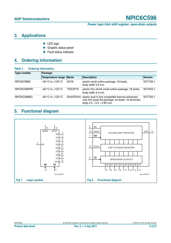
The NPIC6C596 is an 8-bit serial-in/serial or parallel-out shift register with a storage register and open-drain outputs.
Both the shift and storage register have separate clocks.
Features
- Specified from 40 C to +125 C.
- Low RDSon.
- Eight Power EDNMOS transistor outputs of 100 mA continuous current.
- 250 mA current limit capability.
- Output clamping voltage 33 V.
- 30 mJ avalanche energy capability.
- Enhanced cascading for multiple stages.
- All registers cleared with single input.
- Low power consumption.
- ESD protection:.
- HBM JDS-001 Class 2 exceeds 2500 V.
- CDM JESD22-C101E exceeds 1000 V
NXP Semiconductors
NPIC6C596
Power lo.
 NPIC6C596 Datasheet