BU1706AX
Overview
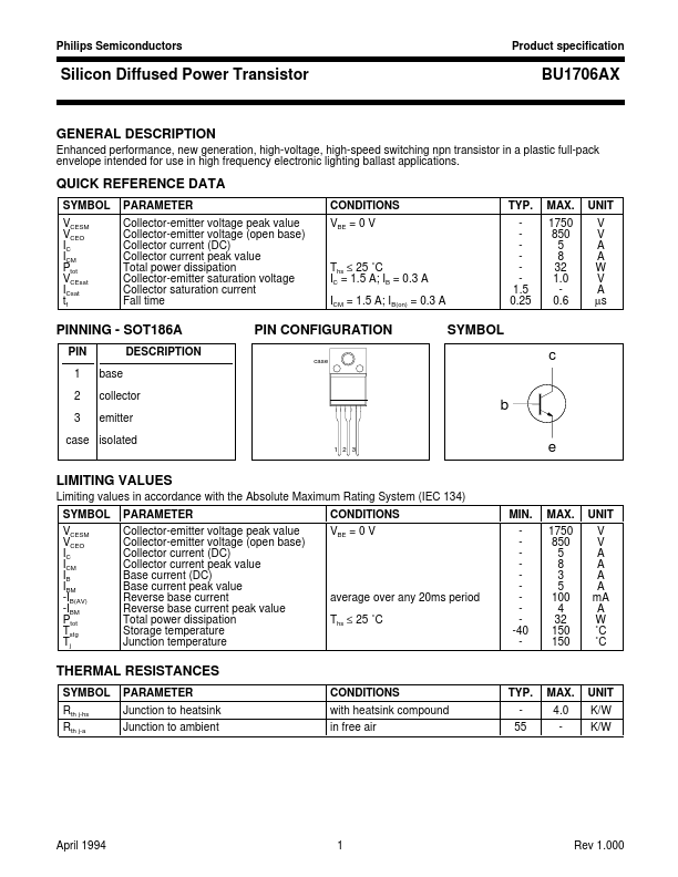
Philips Semiconductors Product specification Silicon Diffused Power Transistor BU1706AX GENERAL DESCRIPTION Enhanced performance, new generation, high-voltage, high-speed switching npn transistor ...
| Part | BU1706AX |
|---|---|
| Description | Silicon Diffused Power Transistor |
| Category | Transistor |
| Manufacturer | NXP Semiconductors |
| Size | 78.02 KB |
Philips Semiconductors Product specification Silicon Diffused Power Transistor BU1706AX GENERAL DESCRIPTION Enhanced performance, new generation, high-voltage, high-speed switching npn transistor ...
| Part Number | Manufacturer | Description |
|---|---|---|
| BU1706AX | Inchange Semiconductor | NPN Transistor |
| BU1706AX | SavantIC | SILICON POWER TRANSISTOR |
| BU1706A | Inchange Semiconductor | NPN Transistor |
| BU17074KV | ROHM | Serial Interface Transceiver LSI |