Datasheet Details
| Part number | 74VHC08 |
|---|---|
| Manufacturer | NXP Semiconductors |
| File Size | 75.06 KB |
| Description | Quad 2-input AND gate |
| Datasheet |
 74VHC08 Datasheet 74VHC08 Datasheet
|
|
|
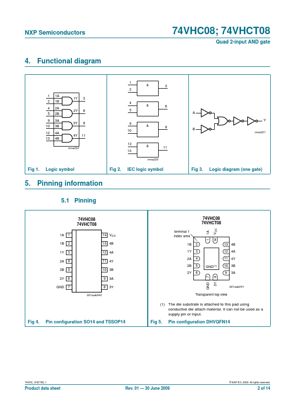
The 74VHC08; 74VHCT08 are high-speed Si-gate CMOS devices and are pin compatible with Low-power Schottky TTL (LSTTL).
They are specified in compliance with JEDEC standard JESD7-A.
The 74VHC08; 74VHCT08 provide the quad 2-input AND function.
| Part number | 74VHC08 |
|---|---|
| Manufacturer | NXP Semiconductors |
| File Size | 75.06 KB |
| Description | Quad 2-input AND gate |
| Datasheet |
74VHC08 Datasheet
|
|
|
|
| Part Number | Description | Manufacturer |
|---|---|---|
| 74VHC08 | QUAD 2-INPUT AND GATE | STMicroelectronics |
| 74VHC08 | Quad 2-Input AND Gate | Fairchild Semiconductor |
| 74VHC08 | Quad 2-Input AND Gate | ON Semiconductor |
| 74VHC08 | Quad 2-input AND gate | nexperia |
| 74VHC08-Q100 | Quad 2-input AND gate | nexperia |
| Part Number | Description |
|---|---|
| 74VHC08-Q100 | Quad 2-input AND gate |
| 74VHC02 | Quad 2-input NOR gate |
| 74VHC02-Q100 | Quad 2-input NOR gate |
| 74VHC125 | Quad buffer/line driver |
| 74VHC126 | Quad buffer/line driver |
The following content is an automatically extracted verbatim text from the original manufacturer datasheet and is provided for reference purposes only.