74LVC126A
Description
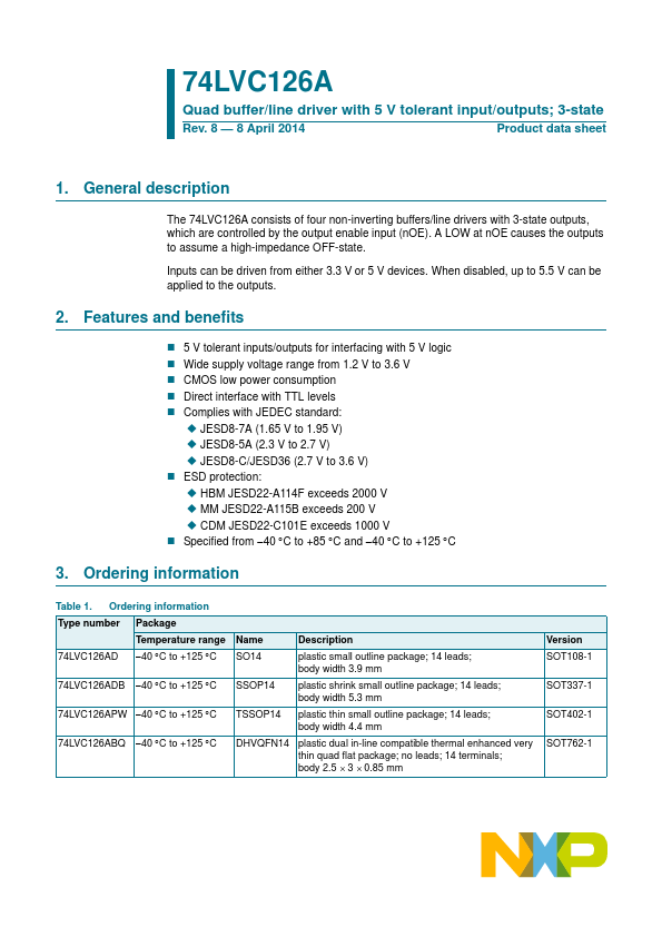
The 74LVC126A consists of four non-inverting buffers/line drivers with 3-state outputs, which are controlled by the output enable input (nOE).
Key Features
- 5 V tolerant inputs/outputs for interfacing with 5 V logic
- Wide supply voltage range from 1.2 V to 3.6 V
- CMOS low power consumption
- Direct interface with TTL levels
- Specified from 40 C to +85 C and 40 C to +12