Datasheet4U Logo Datasheet4U.com

74ALS10A Datasheet Triple 3-Input NAND gate

Manufacturer: NXP Semiconductors

General Description

COMMERCIAL RANGE VCC = 5V ±10%, Tamb = 0°C to +70°C 74ALS10AN 74ALS10AD DRAWING NUMBER 2B 2C 2Y GND 14-pin plastic DIP 14-pin plastic SO SOT27-1 SOT108-1 SC00014 INPUT AND OUTPUT LOADING AND FAN-OUT TABLE PINS nA, nB, nC nY Data inputs Data outputs DESCRIPTION 74ALS (U.L.) HIGH/LOW 1.0/1.0 20/80 LOAD VALUE HIGH/LOW 20µA/0.1mA 0.4mA/8mA NOTE: 
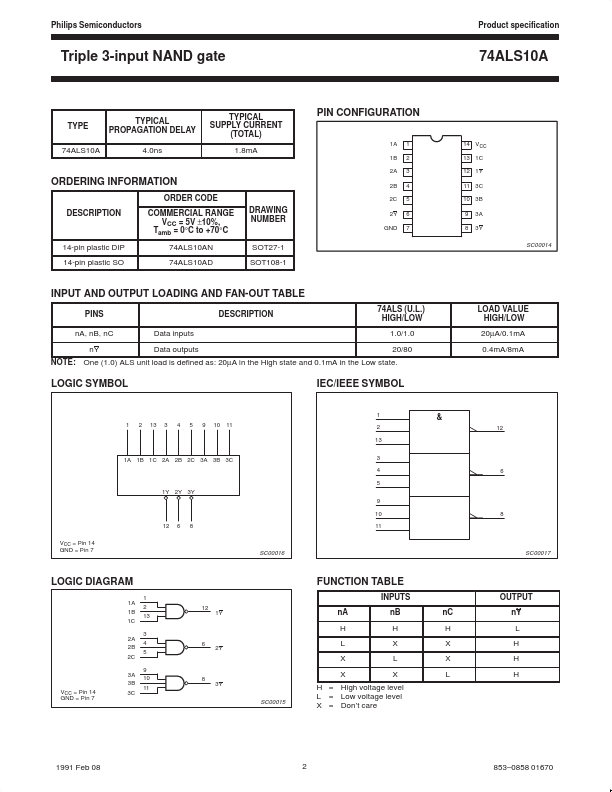
One (1.0) ALS unit load is defined as: 20µA in the High state and 0.1mA in the Low state.

LOGIC SYMBOL IEC/IEEE SYMBOL 1 & 12 1 2 13 3 4 5 9 10 11 2 13 1A 1B 1C 2A 2B 2C 3A 3B 3C 3 4 5 6 1Y 2Y 3Y 9 10 12 VCC = Pin 14 GND = Pin 7 6 8 11 8 SC00016 SC00017 LOGIC DIAGRAM 1A 1B 1C 2A 2B 2C 3A 3B VCC = Pin 14 GND = Pin 7 3C 1 2 13 3 4 5 9 10 11 12 1Y FUNCTION TABLE INPUTS nA H 6 2Y OUTPUT nC H X X L nY L H H H nB H X L X L X 8 X 3Y SC00015 H = High voltage level L = Low voltage level X = Don’t care 1991 Feb 08 2 853–0858 01670 Philips Semiconductors Product specification Triple 3-input NAND gate 74ALS10A ABSOLUTE MAXIMUM RATINGS (Operation beyond the limit set forth in this table may impair the useful life of the device.

Unless otherwise noted these limits are over the operating free-air temperature range.) SYMBOL VCC VIN IIN VOUT IOUT Tamb Tstg Supply voltage Input voltage Input current Voltage applied to output in High output state Current applied to output in Low output state Operating free-air temperature range Storage temperature range PARAMETER RATING –0.5 to +7.0 –0.5 to +7.0 –30 to +5 –0.5 to VCC 16 0 to +70 –65 to +150 UNIT V V mA V mA °C °C RECOMMENDED OPERATING

Overview

INTEGRATED CIRCUITS 74ALS10A Triple 3-Input NAND gate Product specification IC05 Data Handbook 1991 Feb 08 Philips Semiconductors Philips Semiconductors Product specification Triple 3-input NAND gate 74ALS10A TYPE 74ALS10A TYPICAL PROPAGATION DELAY 4.0ns TYPICAL SUPPLY CURRENT (TOTAL) 1.