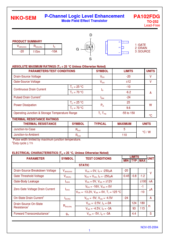
NIKO-SEM P-Channel Logic Level Enhancement
Mode Field Effect Transistor
PA102FDG
TO-252
Lead-Free
DYNAMIC
Input Capacitance
Output Capacitance
Ciss
Coss VGS = 0V, VDS = -6V, f = 1MHz
430
235
Reverse Transfer Capacitance
Total Gate Charge2
Gate-Source Charge2
Gate-Drain Charge2
Turn-On Delay Time2
Rise Time2
Turn-Off Delay Time2
Fall Time2
Crss
Qg
Qgs
Qgd
td(on)
tr
td(off)
tf
VDS = 0.5V(BR)DSS, VGS = -4.5V,
ID = -3A
VDD = -10V
ID ≅ -1A, VGS = -5V, RG = 6
95
7.6 10
3.2
2
25
60
70
60
SOURCE-DRAIN DIODE RATINGS AND CHARACTERISTICS (TC = 25 °C)
Continuous Current
IS
Pulsed Current3
ISM
Forward Voltage1
VSD
1Pulse test : Pulse Width ≤ 300 µsec, Duty Cycle ≤ 2 .
2Independent of operating temperature.
3Pulse width limited by maximum junction temperature.
IF = -10A, VGS = 0V
-10
-24
-1.2
pF
nC
nS
A
V
REMARK: THE PRODUCT MARKED WITH PA102FDG, DATE CODE or LOT #
Orders for parts with Lead-Free plating can be placed using the PXXXXXXG parts name.
NOV-05-2004
2