The following content is an automatically extracted verbatim text
from the original manufacturer datasheet and is provided for reference purposes only.
View original datasheet text
NIKO-SEM
P-Channel Logic Level Enhancement P6010DDG
Mode Field Effect Transistor
TO-252
Halogen-Free & Lead-Free
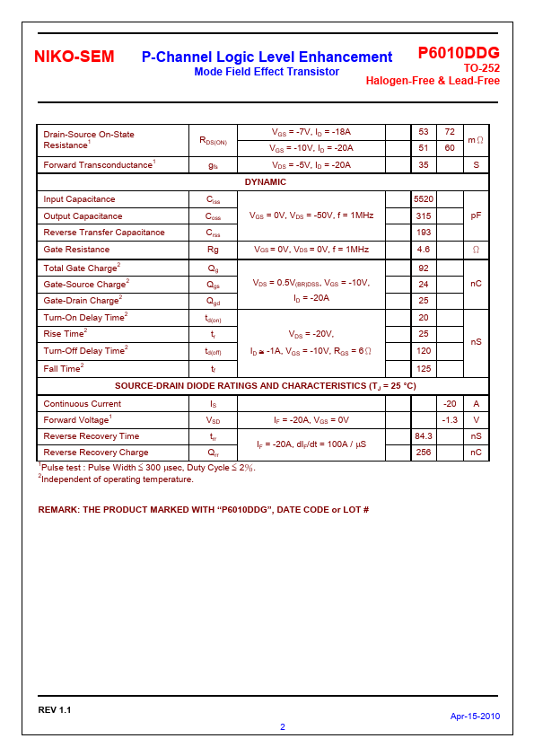
PRODUCT SUMMARY
V(BR)DSS
RDS(ON)
-100V
60mΩ
ID -20A
D G
S
ABSOLUTE MAXIMUM RATINGS (TA = 25 °C Unless Otherwise Noted)
PARAMETERS/TEST CONDITIONS
SYMBOL
Drain-Source Voltage
Gate-Source Voltage
Continuous Drain Current Pulsed Drain Current1
TC = 25 °C TC = 100 °C
Avalanche Current
Avalanche Energy
L = 0.1mH
Power Dissipation
TC = 25 °C TC = 100 °C
Operating Junction & Storage Temperature Range
VDS VGS
ID
IDM IAS EAS
PD
Tj, Tstg
THERMAL RESISTANCE RATINGS THERMAL RESISTANCE
SYMBOL
TYPICAL
Junction-to-Case
RθJc
Junction-to-Ambient
RθJA
1Pulse width limited by maximum junction temperature.
1. GATE 2. DRAIN 3.
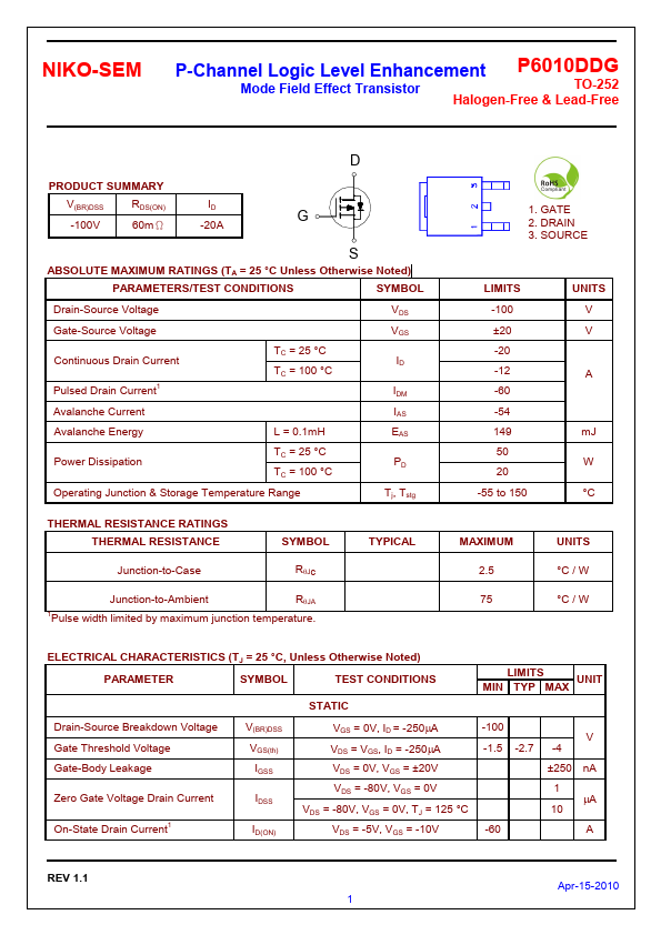
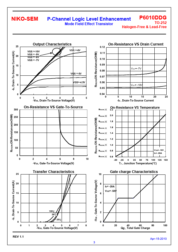
 P6010DDG Datasheet