Datasheet Details
| Part number | P2610ASG |
|---|---|
| Manufacturer | NIKO-SEM |
| File Size | 192.54 KB |
| Description | N-Channel MOSFET |
| Datasheet |
 P2610ASG Datasheet P2610ASG Datasheet
|
|
|
Download the P2610ASG datasheet PDF. This datasheet also covers the P2610ASG-NIKO variant, as both devices belong to the same n-channel mosfet family and are provided as variant models within a single manufacturer datasheet.
| Part number | P2610ASG |
|---|---|
| Manufacturer | NIKO-SEM |
| File Size | 192.54 KB |
| Description | N-Channel MOSFET |
| Datasheet |
P2610ASG Datasheet
|
|
|
|
| Part Number | Description | Manufacturer |
|---|---|---|
| P2610ADG | N-Channel Transistor | UNIKC |
| P2610AI | MOSFET | UNIKC |
| P2610ATFG | N-Channel MOSFET | UNIKC |
| P2610ATG | N-Channel MOSFET | UNIKC |
| P2610BD | N-Channel Transistor | UNIKC |
| Part Number | Description |
|---|---|
| P2610ADG | N-Channel Transistor |
| P2610BT | N-Channel Transistor |
| P2610BTF | N-Channel Transistor |
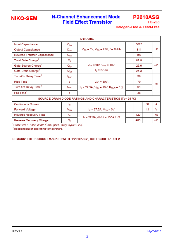
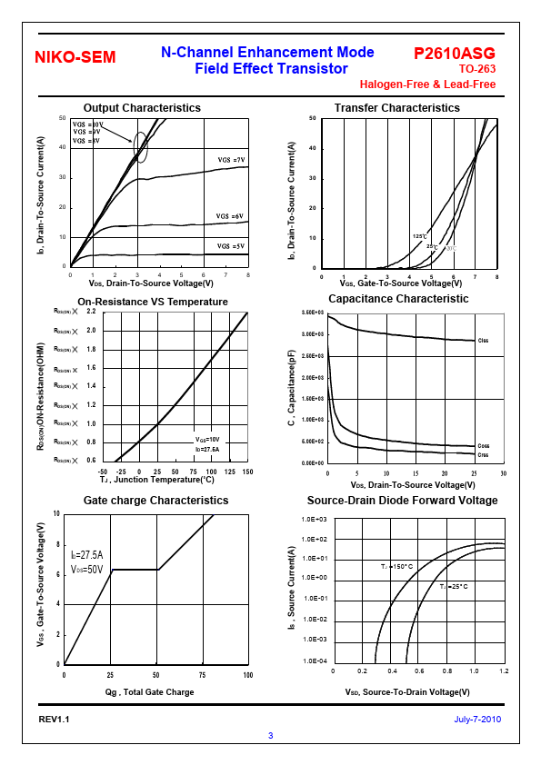
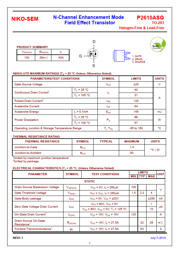
The following content is an automatically extracted verbatim text from the original manufacturer datasheet and is provided for reference purposes only.