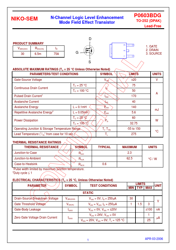
P0603BDG
P0603BDG is N-Channel MOSFET manufactured by NIKO-SEM.
- Part of the P0603BDG-NIKO comparator family.
- Part of the P0603BDG-NIKO comparator family.
NIKO-SEM
N-Channel Logic Level Enhancement Mode Field Effect Transistor
TO-252 (DPAK) Lead-Free
PRODUCT SUMMARY V(BR)DSS 30 RDS(ON) 6.5m ID 75A 1. GATE 2. DRAIN 3. SOURCE
ABSOLUTE MAXIMUM RATINGS (TC = 25 °C Unless Otherwise Noted) PARAMETERS/TEST CONDITIONS Gate-Source Voltage Continuous Drain Current Pulsed Drain Current Avalanche Current Avalanche Energy Repetitive Avalanche Energy Power Dissipation
2 1
SYMBOL VGS
LIMITS ±20 75 50 170 40 140 5.6 60 32.75 -55 to 150 275
UNITS V
TC = 25 °C TC = 100 °C
ID IDM IAS
L = 0.1m H L = 0.05m H TC = 25 °C TC = 100 °C
EAS EAR PD Tj, Tstg TL m J
Operating Junction & Storage Temperature Range Lead Temperature ( /16” from case for 10 sec.) THERMAL RESISTANCE RATINGS THERMAL RESISTANCE Junction-to-Case Junction-to-Ambient Case-to-Heatsink
1 2 1
°C
SYMBOL RθJC RθJA RθCS
TYPICAL
MAXIMUM 2.3 62.5
UNITS
°C / W
Pulse width limited by maximum junction temperature. Duty cycle ≤ 1
ELECTRICAL CHARACTERISTICS (TC = 25 °C, Unless Otherwise Noted) PARAMETER SYMBOL TEST CONDITIONS STATIC Drain-Source Breakdown Voltage Gate Threshold Voltage Gate-Body Leakage Zero Gate Voltage Drain Current V(BR)DSS VGS(th) IGSS IDSS VGS = 0V, ID = 250µA VDS = VGS, ID = 250µA VDS = 0V, VGS = ±20V VDS = 24V, VGS = 0V VDS = 20V, VGS = 0V, TJ = 125 °C 30 1 1.5 3 ±100 1 25 n A µA V LIMITS UNIT MIN TYP MAX
APR-03-2006
NIKO-SEM
On-State Drain Current1 Drain-Source On-State Resistance1
N-Channel Logic Level Enhancement Mode Field Effect Transistor
TO-252 (DPAK) Lead-Free
70 5.3 7.6 19 6.5 9.5 A m S
ID(ON) RDS(ON) gfs
VDS = 10V, VGS = 10V VGS = 10V, ID = 30A VGS = 5V, ID = 24A VDS = 15V, ID = 30A DYNAMIC
Forward Transconductance1
Input Capacitance Output Capacitance Reverse Transfer Capacitance Total Gate Charge2 Gate-Source Charge Gate-Drain Charge2 Turn-On Delay Time Rise Time
2 2...