The following content is an automatically extracted verbatim text
from the original manufacturer datasheet and is provided for reference purposes only.
View original datasheet text
PNP Medium Power Transistor
Features:
• PNP Silicon Power Switching Transistors • Medium Power Amplifier and Switching Applications
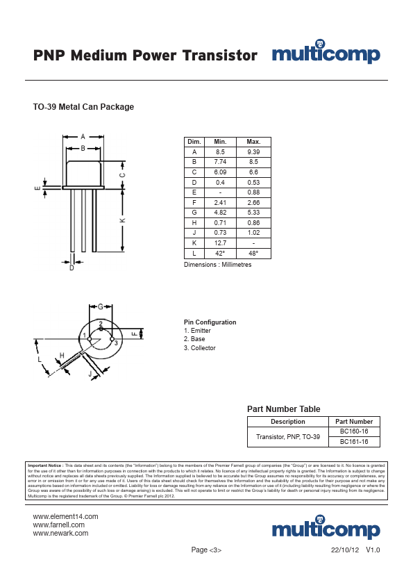
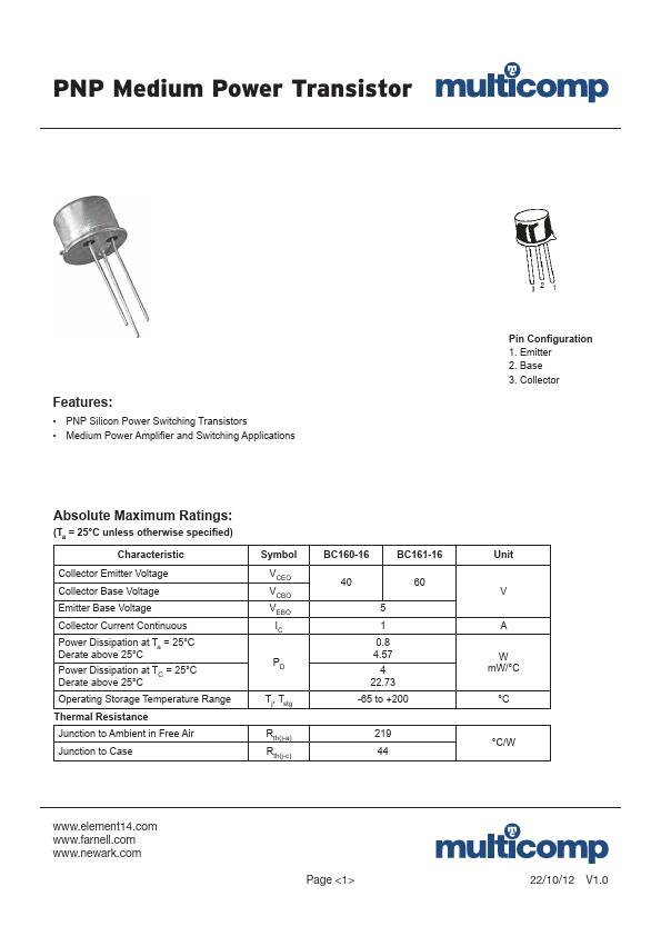
Pin Configuration 1. Emitter 2. Base 3. Collector
Absolute Maximum Ratings:
(Ta = 25°C unless otherwise specified)
Characteristic Collector Emitter Voltage Collector Base Voltage Emitter Base Voltage Collector Current Continuous Power Dissipation at Ta = 25°C Derate above 25°C Power Dissipation at TC = 25°C Derate above 25°C Operating Storage Temperature Range Thermal Resistance Junction to Ambient in Free Air Junction to Case
Symbol VCEO VCBO VEBO IC
PD
Tj, Tstg
Rth(j-a) Rth(j-c)
BC160-16
BC161-16
40 60
5
1
0.8 4.57
4 22.73
-65 to +200
219 44
Unit
V A W mW/°C °C
°C/W
www.element14.com www.farnell.com www.newark.com
Page <1>
22/10/12 V1.
 BC160-16 Datasheet